
In this article we will be taking a look at the onboard external flash that comes on the Tang Nano9K. The onboard flash provides a whopping 4MB of storage which is both useful for applications where you need a lot of data, or even in applications where you simply want to store persistent data which will not be erased on power off.
Covering both reading and writing to flash would make this article a bit long, so in this part we will focus on exploring the flash chip and reading data from it and in the next section we will go over writing to the flash chip persisting data in your application.
The Plan
To showcase reading data off the flash chip we will be building a hex viewer where we can display on screen a section of memory in hex format and have the ability to traverse through the different memory addresses using the on-board buttons.
We will be using some modules we built in the past like our screen module and text engine so we have the ability to write text to the screen.
But before we get ahead of ourselves let's take a look at the IC in question.
The P25Q32U IC
Taking a look at the Tang Nano 9K schematic we can see we have something titled "SPI Flash":
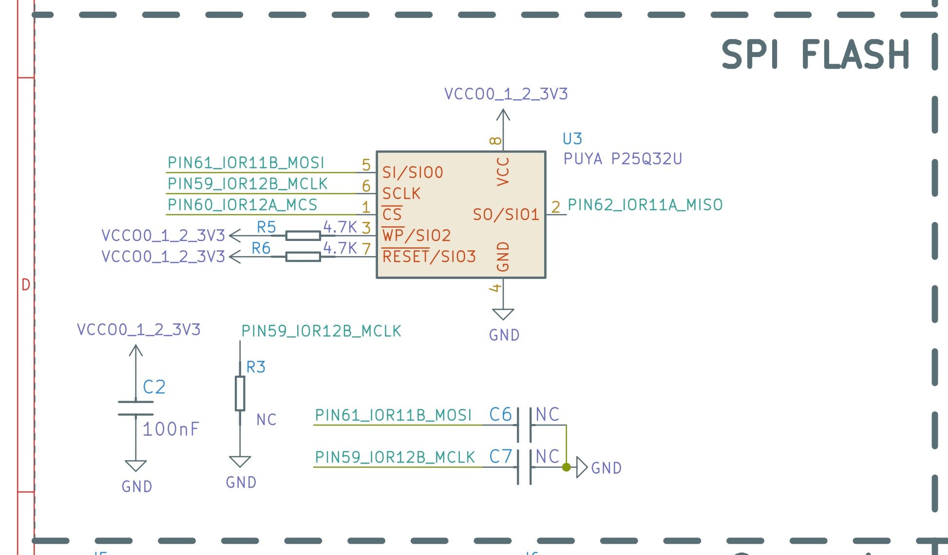
First off we can see the IC used: "Puya P25Q32U", besides for that we can see that we are using standard SPI with 4 pins.
The ICs datasheet:
Taking a look at the ICs datasheet we can see that it is a 32M-bit flash IC which is a nice way of saying 4MB.
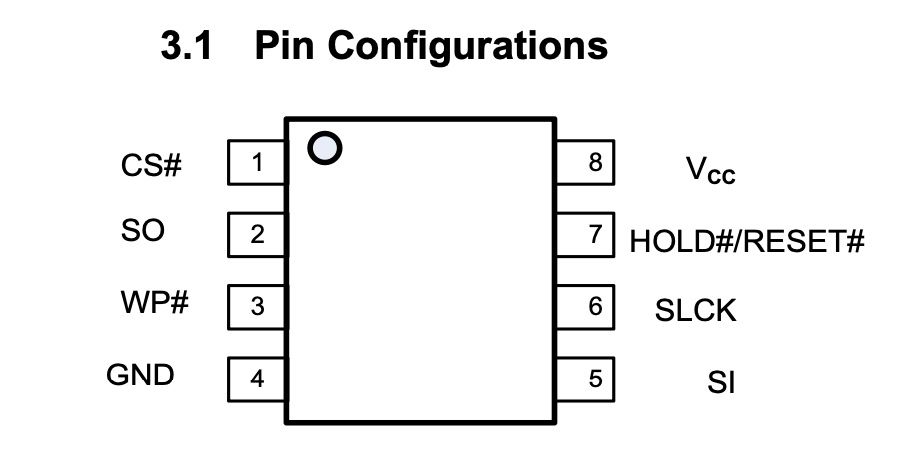
Taking a look at the pinout we can see that besides the SPI pins the IC has a write protection pin which is active low, and a reset pin which is also active low. From the Tang Nano schematic we can see these two have been pulled high through a resistor so the chip allows writing to and will never be hardware reset.
We won't go through the whole datasheet but to go over some of the highlights:
- 24-bit address from 000000 to 3FFFFF in hex to access all 4 megabyte.
- Each address points at a single byte.
- The bytes are reset to FF not 00.
There are also some more advanced features like locking certain areas of memory or clearing the entire memory in a single operation but we won't be covering those features.
We can also see the IC supports multiple communication methods like SPI, Dual SPI, Quad SPI, etc. but from the tang nano 9K schematic we can see we only have a single SPI connection so only the standard SPI is relevant.
Chapter 10 has the commands table where you can get an overview of the commands offered. In this article we will be focusing on the read command.
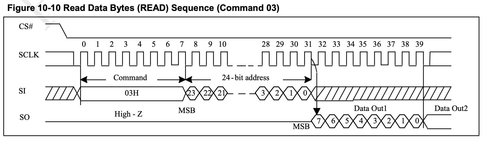
We can see we have to set the chip select to low since it's active low, we then send the command, changing the bit on the MOSI pin on the falling edge and the command will be read on the rising edge.
After sending the command we send 24 bits representing the address and then we need to pulse the clock another 8 times for each byte we want to read. The flash chip will continue to output bytes in order for as many as we want, we can even read the full memory from a single read command. To stop reading we need to set the CS pin back high to stop the transmission.
In our example since our screen can display a total of 64 characters (4 rows of 16) and each byte takes up two characters in hex, we will be reading 32 bytes so we can fill the entire screen each time we read data.
We can also see from the datasheet that their is a bit of time required after power up to make sure the IC has initialized. There is a status flag we could check to make sure the chip is up, but we will just wait a fixed period where we can be sure it will be ready.
Other then that we can see from Chapter 5.3 that the max frequency for reading is 33Mhz which is above our 27Mhz oscillator on the tang nano and their is no minimum speed so we don't have any special requirements to take into consideration in terms of speeds.
We now have everything we need in terms of info to start developing our hex viewer.
The Flash Navigator
Let's get straight into developing the flash navigator. To begin with we won't worry about the navigation part, let us just see we can read 32 bytes of memory from the flash IC.
Create a file in a new directory called flash.v :
module flashNavigator
#(
  parameter STARTUP_WAIT = 32'd10000000
)
(
    input clk,
    output reg flashClk = 0,
    input flashMiso,
    output reg flashMosi = 0,
    output reg flashCs = 1,
    input [5:0] charAddress,
    output reg [7:0] charOutput = 0,
    input btn1,
    input btn2
);


endmodule
Our module needs to receive the wait time for the flash to initialize as a parameter. For inputs / outputs we have the following:
clk- the 27Mhz main clock signal.flashClk- the SPI clock for the flash IC.flashMiso- the SPI data in from the flash to the tang nano.flashMosi- the SPI data out from the tang nano to flash.flashCs- the SPI chip select, active low.charAddress- the current char to display to the screen (used to interface with the text engine).charOutput- the character in ASCII format that we want to be displayed atcharAddress.btn1/btn2- the two buttons on the tang nano board.
For all the outputs we add the reg keyword to make it auto generate an output register connected to those wires. Next we can create some registers:
  reg [23:0] readAddress = 0;
  reg [7:0] command = 8'h03;
  reg [7:0] currentByteOut = 0;
  reg [7:0] currentByteNum = 0;
  reg [255:0] dataIn = 0;
  reg [255:0] dataInBuffer = 0;
readAddress is a register to store the 24-bit address we want to read from flash, command stores the command we want to send the flash IC, 03 is the READ command as we saw in the datasheet.
Next we need a register to store the current data byte from flash (currentByteOut), as well as a counter to count which byte we are on from the 32 bytes we want to read (currentByteNum). Finally we have two buffers which are 256 bits long or 32 bytes to hold a single read operation of 32 bytes.
The reason we have a separate register for the entire 32 bytes and a separate register for the current bit is just because it sends each byte MSB first, but the bytes come least significant byte first so they have apposing directions if we wanted to shift the data in. We would have to jump 8 bits forward and then backtrack when updating the memory which would make the code more complex.
So by separating them we can shift the current byte in by shifting the MSB left and then just add it to the dataIn register which stores the entire frame.
The reason we have two buffers for the current frame is so that one will be controlled by the reading code and one will be used by the other components consuming the data. This way we don't have to synchronize between them we simply read bits into dataIn and only when we have a complete frame we update dataInBuffer all at once so components consuming the data always have an up to date frame they can read from.
Next our flash navigator module will have the following states to perform the read sequence:
  localparam STATE_INIT_POWER = 8'd0;
  localparam STATE_LOAD_CMD_TO_SEND = 8'd1;
  localparam STATE_SEND = 8'd2;
  localparam STATE_LOAD_ADDRESS_TO_SEND = 8'd3;
  localparam STATE_READ_DATA = 8'd4;
  localparam STATE_DONE = 8'd5;
We will wait for the IC to initialize, then load the command we want to send, we can then send the command in the state STATE_SEND. After sending the command we need to send the address, this can be done by loading the address and reusing the same STATE_SEND state to send the loaded register.
After sending both the command to read and address we want, we need to read 32 bytes out, this can be done in the STATE_READ_DATA state. Once all 32 bytes are read we will go to the done state and transfer our dataIn register into dataInBuffer.
To accomplish this we will need a few more registers:
  reg [23:0] dataToSend = 0;
  reg [8:0] bitsToSend = 0;

  reg [32:0] counter = 0;
  reg [2:0] state = 0;
  reg [2:0] returnState = 0;

  reg dataReady = 0;
Since we will be using the same send state for both sending the command as-well as the address, we create another common register which we can store either the command or address and then the send state only needs to send from here.
bitsToSend is the number of bits we want to send, since commands are only 8 bits long and addresses 24 we have to know how many we want each time we are sending data.
counter is a general purpose counter register we will use in our state machine, state stores our current state and returnState is the state to return to after sending data. This is again because we are using the send state for two different parts of the read sequence so we have to know where to return to.
The final register is a 1 bit flag which will be set high once we have finished reading all 32 bytes to tell other parts of the module when it can use the data.
Next lets add an always block and start implementing our state machine:
  always @(posedge clk) begin
      case (state)
  	      // state machine here
      endcase
  end
The State Machine
We have 6 states in-order to implement the full read sequence, this will be pretty similar to the screen module we made as both are SPI but here we are communicating in both directions, we have to send the command and address and then read data back from the flash chip.
The Power Initialization State
STATE_INIT_POWER: begin
    if (counter > STARTUP_WAIT) begin
        state <= STATE_LOAD_CMD_TO_SEND;
        counter <= 32'b0;
        currentByteNum <= 0;
        currentByteOut <= 0;
    end
    else
        counter <= counter + 1;
end
The first state increments the counter until we reach the desired startup delay in which case it will clear some registers and move onto loading the command to send in the next state.
The Load Command State
STATE_LOAD_CMD_TO_SEND: begin
    flashCs <= 0;
    dataToSend[23-:8] <= command;
    bitsToSend <= 8;
    state <= STATE_SEND;
    returnState <= STATE_LOAD_ADDRESS_TO_SEND;
end
In this state we set the chip select low to activate the flash chip as we are about to start sending data to it as per the datasheet. Other then that we load the command into the send buffer, set the number of bits to send to 8 since our command is 8 bits, and move onto the send state. The last line sets the return state after sending data to be load address state so once it finishes sending the command it will go there.
One thing to notice is we put the command at the top 8 bits instead of the bottom 8 bits from the 24-bit dataToSend register. This is because with this flash chip we are sending MSB first so by putting it at the top 8 bits we can easily shift them off the end.
The Send State
STATE_SEND: begin
    if (counter == 32'd0) begin
        flashClk <= 0;
        flashMosi <= dataToSend[23];
        dataToSend <= {dataToSend[22:0],1'b0};
        bitsToSend <= bitsToSend - 1;
        counter <= 1;
    end
    else begin
        counter <= 32'd0;
        flashClk <= 1;
        if (bitsToSend == 0)
            state <= returnState;
    end
end
Like with our screen module we will be splitting our main clock into two SPI clocks, this is to simplify the code a bit, theoretically we can set the data on the falling edge of the clock and have it read on the rising edge doubling our transfer rate. But to keep everything together we perform the rising and falling edge of the SPI clock in the rising edge of our main clock.
So when the counter is 0 we set the clock low performing the "falling edge" of the spi clock and when the counter is 1 we set the SPI clock high letting the flash chip read the data we set.
On the falling edge we set the output pin to be the most significant bit of dataToSend and then we shift dataToSend one bit to the left since we already handled the last bit. We also decrement bitsToSend and set the counter to 1 so we can move onto the rising edge in the next clock cycle.
On the rising edge, besides for setting the spi clock high and resetting counter we are also checking if this was the last bit in which case we move onto the next state which was stored in returnState
The Load Address State
STATE_LOAD_ADDRESS_TO_SEND: begin
    dataToSend <= readAddress;
    bitsToSend <= 24;
    state <= STATE_SEND;
    returnState <= STATE_READ_DATA;
    currentByteNum <= 0;
end
The load address state is very similar to loading a command except that the register is 24 bits long, we also set the return state to read data, as we saw from the datasheet after sending the address the flash will start outputting the data which we need to read.
The Read Data State
STATE_READ_DATA: begin
    if (counter[0] == 1'd0) begin
        flashClk <= 0;
        counter <= counter + 1;
        if (counter[3:0] == 0 && counter > 0) begin
            dataIn[(currentByteNum << 3)+:8] <= currentByteOut;
            currentByteNum <= currentByteNum + 1;
            if (currentByteNum == 31)
                state <= STATE_DONE;
        end
    end
    else begin
        flashClk <= 1;
        currentByteOut <= {currentByteOut[6:0], flashMiso};
        counter <= counter + 1;
    end
end
The read data state is almost like the flip side of the send data, here we also split our clock into one cycle for the rising edge and one cycle for the falling edge of the SPI clock. The main difference being that when sending data we didn't really care about individual bytes, in both the case of sending 1 byte for the command or 3 bytes for the address we simply had to shift the bytes MSB first from start to end in order.
In the case of reading data, like mentioned above, each byte is read most significant bit first, but the bytes themselves are arranged least significant byte first (or at least lowest address first). So because of these two different directions we will be reading each byte separately and only after reading a full byte we will place it into the final input buffer.
Because of this we need to be able to count each time we have read 8 bits so we will be using counter for this as well, besides for just counting whether or not we are on the rising or falling edge.
So in the top if section where we handle the falling edge, we check if the last 4 bits equal zero, which is another way of saying we have no remainder when dividing by 16 (8 bits * 2 clock cycles per bit) then we know we have read a full byte and we store currentByteOut into the dataIn register. The index where we store it is the currentByteNum multiplied by 8 which is like shifting by 3.
Besides for that we increment the number of bytes read and check if we are already on 31 bytes read and we just incremented the counter then we have finished reading all 32 bytes so we move onto the done state.
In the else block where we handle the rising edge of the SPI clock we read the current bit from flashMosi and shift it into the currentByteOut register. Since the data is sent MSB first we shift left, so that after 8 shifts the first bit we put in will be the most significant bit.
The Done State
STATE_DONE: begin
    dataReady <= 1;
    flashCs <= 1;
    dataInBuffer <= dataIn;
    counter <= STARTUP_WAIT;
    state <= STATE_INIT_POWER;
end
Our final state turns off the flash chip by setting the chip select pin high stopping the read operation and we copy the data read from dataIn to dataInBuffer making the new data available to other components to use. We set the dataReady flag to 1 to tell other components that the register dataInBuffer contains the contents from flash for the address requested.
We also reset counter to be the startup delay and go back to the first state to repeat the cycle but this time without a delay.
With that we should now be able to read the first 32 bytes of memory.
Displaying The Data
Having the data read is nice, but we need to be able to see it to believe it. So let's add to the same flashNavigator module some code to output the data in hex format to the screen.
We can copy our toHex converter module (to the same file flash.v) we used in the previous article:
module toHex(
    input clk,
    input [3:0] value,
    output reg [7:0] hexChar = "0"
);
    always @(posedge clk) begin
        hexChar <= (value <= 9) ? 8'd48 + value : 8'd55 + value;
    end
endmodule
Which takes in a 4-bit number and converts it to a hex letter in ASCII format. We can then add the following to our flashNavigator module:
reg [7:0] chosenByte = 0;

wire [7:0] byteDisplayNumber;
wire lowerBit;

wire [7:0] hexCharOutput;
wire [3:0] currentHexVal;
chosenByte will store the current byte we want to display from the 32 different bytes we have read from memory. byteDisplayNumber will be the index of the byte we want so again this can be from 0-31. Each byte is represented by 2 hex characters so we need to know if we are on the first or second character which we do with lowerBit.
Finally hexCharOutput will store the ASCII value we get back from the hex conversion and currentHexVal will store the 4 bits we are currently converting.
Let's take a look at how to hook that up:
assign byteDisplayNumber = charAddress[5:1];
assign lowerBit = charAddress[0];
assign currentHexVal = lowerBit ? chosenByte[3:0] : chosenByte[7:4];

toHex hexConvert(
    clk,
    currentHexVal,
    hexCharOutput
);
As each byte is represented by 2 characters we can take the character address and divide by 2 to get the byte index. Dividing by two is like shifting right or simply removing the smallest bit, so we put that into byteDisplayNumber.
lowerBit is every second character we are printing the lower bit of a byte, so we only need to check if the LSB is 1 then we are on a second character.
Based on whether or not we are on the higher half or lower half of the byte we take the corresponding 4 bits out of the 8 bit byte chosenByte and put that into currentHexVal.
The last block creates an instance of our hex converter with the current 4-bits we want to convert and it will output the result to hexCharOutput.
The only thing we have left to do is to put the current data we want to convert into chosenByte and output hexCharOutput back to the text engine to convert to pixel data.
always @(posedge clk) begin
    chosenByte <= dataInBuffer[(byteDisplayNumber << 3)+:8];
    charOutput <= hexCharOutput;
end
We don't really need to check the dataReady flag since we have a double buffer for the input data we always have a valid frame which we can display while the read sequence continues to update the other register.
It is worth noting byteDisplayNumber only holds the byte number which has a max value of 31, but we still made it 8 bits instead of 5, and that is because we are shifting it 3 places left in the always block. It is something that you have to pay attention to, but if we made it 5 bits long and shifted it 3 times, we would only have 2 bits left as anything shifted over the 5th bit position would be lost, resulting in an index which would cycle between 4 values (00000, 01000, 10000,11000) as the 3 smallest bits will always be zero (since we just shifted them in) and anything over the 5th bit would be cutoff. To fix this we need to make the register 8 bits long to be able to hold the full value after shifting it.
We should now have a complete module which allows us to load the first 32 bytes and display them to the screen. To test it though we need to do a bit of setup.
Project Setup
Besides the flash.v file we need a few other files in-order to run our project, first-off we have the constraints file which defines all the pins we used. Create a file called tangnano9k.cst with the following:
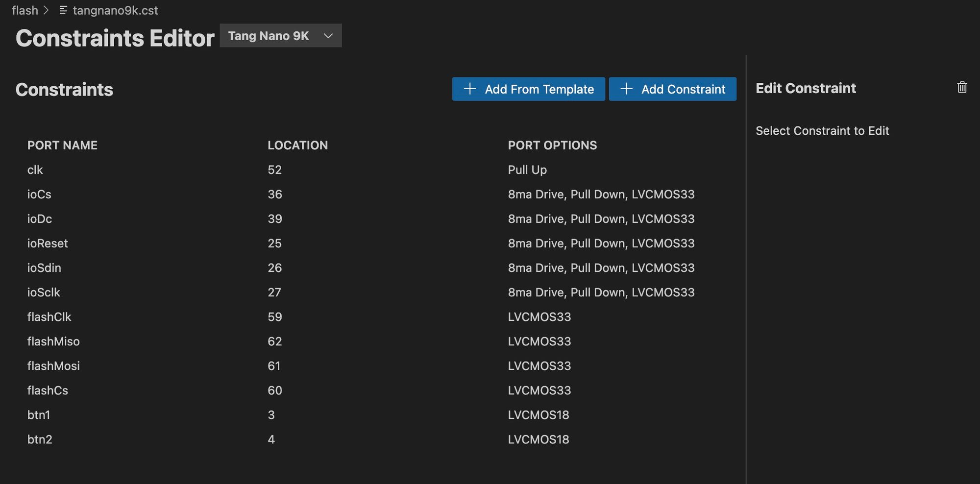
The clock, flash pins and buttons can be imported via the "Add from Template" button and other then that you need to add the constraints for the OLED screen. If doing this manually it would look something like this:
IO_LOC "clk" 52;
IO_PORT "clk" PULL_MODE=UP;

IO_LOC "ioCs" 36;
IO_PORT "ioCs" IO_TYPE=LVCMOS33 PULL_MODE=DOWN DRIVE=8;
IO_LOC "ioDc" 39;
IO_PORT "ioDc" IO_TYPE=LVCMOS33 PULL_MODE=DOWN DRIVE=8;
IO_LOC "ioReset" 25;
IO_PORT "ioReset" IO_TYPE=LVCMOS33 PULL_MODE=DOWN DRIVE=8;
IO_LOC "ioSdin" 26;
IO_PORT "ioSdin" IO_TYPE=LVCMOS33 PULL_MODE=DOWN DRIVE=8;
IO_LOC "ioSclk" 27;
IO_PORT "ioSclk" IO_TYPE=LVCMOS33 PULL_MODE=DOWN DRIVE=8;

IO_LOC "flashClk" 59;
IO_PORT "flashClk" IO_TYPE=LVCMOS33;
IO_LOC "flashMiso" 62;
IO_PORT "flashMiso" IO_TYPE=LVCMOS33;
IO_LOC "flashMosi" 61;
IO_PORT "flashMosi" IO_TYPE=LVCMOS33;
IO_LOC "flashCs" 60;
IO_PORT "flashCs" IO_TYPE=LVCMOS33;

IO_LOC "btn1" 3;
IO_PORT "btn1" IO_TYPE=LVCMOS18;
IO_LOC "btn2" 4;
IO_PORT "btn2" IO_TYPE=LVCMOS18;
We have the clock, the SPI pins for the OLED screen, the SPI pins for the flash IC and the two on-board buttons. The pin numbers were all taken from the tang nano board schematic.
Next we need the screen.v , text.v and font file (font.hex) from our previous project which include the text engine and screen driver for the OLED panel. You can find these in the github repo here, along with the full article describing the build process at these two links: screen, text engine.
Next we need a top module which will connect all our other modules. Create a file called top.v with the following:
module top
#(
  parameter STARTUP_WAIT = 32'd10000000
)
(
    input clk,
    output ioSclk,
    output ioSdin,
    output ioCs,
    output ioDc,
    output ioReset,
    output flashClk,
    input flashMiso,
    output flashMosi,
    output flashCs,
    input btn1,
    input btn2,
);
    wire [9:0] pixelAddress;
    wire [7:0] textPixelData;
    wire [5:0] charAddress;
    wire [7:0] charOutput;

    reg btn1Reg = 1, btn2Reg = 1;
    always @(negedge clk) begin
        btn1Reg <= btn1 ? 1 : 0;
        btn2Reg <= btn2 ? 1 : 0;
    end

    screen #(STARTUP_WAIT) scr(
        clk,
        ioSclk,
        ioSdin,
        ioCs,
        ioDc,
        ioReset,
        pixelAddress,
        textPixelData
    );

    textEngine te(
        clk,
        pixelAddress,
        textPixelData,
        charAddress,
        charOutput
    );

    flashNavigator externalFlash(
        clk,
        flashClk,
        flashMiso,
        flashMosi,
        flashCs,
        charAddress,
        charOutput,
        btn1Reg,
        btn2Reg
    );
endmodule
The top module receives all the inputs and outputs from the constraints file and instantiates all the other modules wiring them up. We have the basic setup for our screen driver and text engine.
Just as a recap, the screen iterates over all pixels on screen in 1024 bytes. Each time it requests a single byte using the pixelAddress register. The text engine takes this pixel address and converts it into a character index by splitting the screens pixels into 4 rows of 16 characters.
The flashNavigator takes this character index and decides which of the 32 bytes we read from memory we want to display and which of its two hex characters for the current byte we need to display. The ASCII result is sent back to the text engine using the charOutput wire which the text engine then converts to individual pixels which the screen needs in-order to draw the current pixels. This is done with textPixelData.
Another thing that is important to note, is that the buttons are on the 1.8V bank and the flash chip is in the 3.3V bank. Connecting these two banks (by using them in the same expression or connecting each to the same registers) will cause a compilation error while generating the bitstream as to not accidentally mix the different voltage levels. To get around this we can do something like the following:
reg btn1Reg = 1, btn2Reg = 1;
always @(negedge clk) begin
    btn1Reg <= btn1 ? 1 : 0;
    btn2Reg <= btn2 ? 1 : 0;
end
Here we create a register for each of the buttons and we don't assign the button directly to the register (making the register also connect to the 1.8V bank) but instead we use the button value to multiplex a separate value into the register. By multiplexing a separate 1 / 0 into the register it lets nextPnR separate the two banks and we won't need to worry about mixing signals.
If you are using the Lushay Code plugin then you are now good to go, if running the OSS toolchain manually then it is also worth creating a Makefile to automate the process:
BOARD=tangnano9k
FAMILY=GW1N-9C
DEVICE=GW1NR-LV9QN88PC6/I5

all: flash.fs

# Synthesis
flash.json: top.v text.v screen.v flash.v
	yosys -p "read_verilog screen.v flash.v text.v top.v; synth_gowin -noalu -top top -json flash.json"

# Place and Route
flash_pnr.json: flash.json
	nextpnr-gowin --json flash.json --write flash_pnr.json --enable-auto-longwires --enable-globals --freq 27 --device ${DEVICE} --family ${FAMILY} --cst ${BOARD}.cst

# Generate Bitstream
flash.fs: flash_pnr.json
	gowin_pack -d ${FAMILY} -o flash.fs flash_pnr.json

# Program Board
load: flash.fs
	openFPGALoader -b ${BOARD} flash.fs -f

# Generate Font
font: font.hex
font.hex:
	node ./scripts/generate_font.js

# Cleanup build artifacts
clean:
	rm flash.fs

.PHONY: load clean test
.INTERMEDIATE: flash_pnr.json flash.json
Like in all our articles this template allows us to run make to run the full toolchain (synthesis, place & route, bitstream generation) and we have make load which will do all the above if needed and also program the FPGA board. Again if using the lushay code plugin this can be skipped and these operations are available through the "FPGA Toolchain" button on the bottom bar.
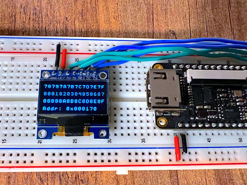
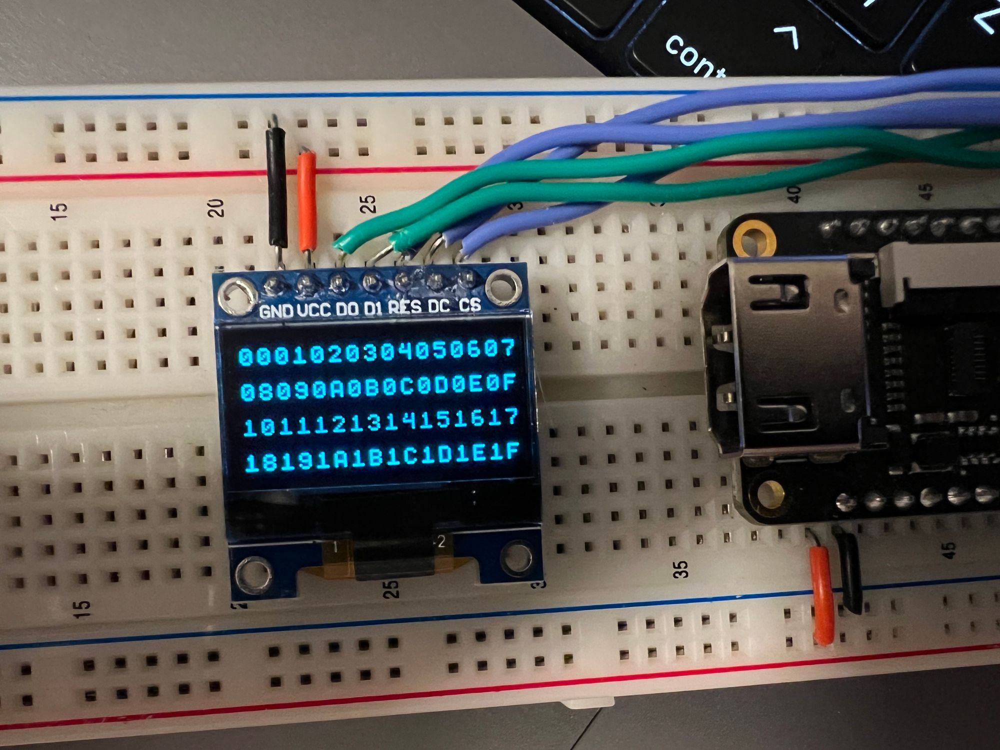
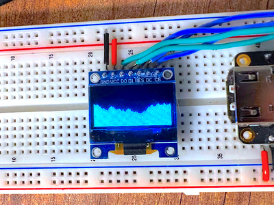
Running the project now should give you a screen full of FFs something like the following:
This is due to the fact that the flash IC resets data to FF like we saw in the datasheet, and since we haven't placed anything into the external flash yet this is what is currently stored there.
Let's take a look now at how we can program something into the external flash.
Programming The External Flash
One of the main advantage of having a large 4MB flash IC on board is the ability to store large amounts of data like look up tables with application specific data or to save on expensive operations, it can also store images / text etc.
To program the flash we can use openFPGALoader with the additional --external-flash flag. But we first need a binary file with the bytes we want to program in.
If all you want to program is a single file, like a text file or image file then you can simply use it. For example if you have a text file called "test.txt" you can program it to the external flash with the following command:
openFPGALoader -b tangnano9k --external-flash test.txtThis can also be done through the Lushay Code plugin, by creating a project file for example flash.lushay.json with the following:
{
    "name": "flash",
    "externalFlashFiles": ["test.txt"]
}
This will add the "External Flash" option when pressing on the "FPGA Toolchain" button, you can also add more files here and then you will be able to choose which one you currently would like to flash.
It is also worth selecting the project file using the button labeled "<Auto-detect Project>" which is next to the "FPGA Toolchain" button, this will make sure code linting is setup.
For our example let's go over how we would create a binary file with node.js which gives us a bit more control over the actual bytes. This would let us define exactly what each of the 4MB will equal.
We can simply create an array of number each 0-255 representing a single byte and then write this to a file as a binary array (buffer).
Here is an example script which adds 256 bytes with the values 0-255 so that we can test our hex viewer to see that all the bytes are converted well. Create a file called generate_bin.js with the following:
const fs = require('fs');

const fileBytes = [];
for (let i = 0; i < 256; i += 1) {
    fileBytes.push(i);
}

fs.writeFileSync('numbers.bin', Buffer.from(fileBytes));
The first line imports the file-system library in-order to write files. We then create an array for all the bytes. Next is a for-loop which has 256 iterations incrementing i from 0 to 255. Each iteration we store i itself as the byte we want to store.
The last line writes the data to a file called numbers.bin converting the array of numbers to a buffer which represents binary data.
Running this script with node generate_bin.js should generate the numbers.bin file. We can then program this file to the external flash by modifying or project file:
{
    "name": "flash",
    "externalFlashFiles": ["numbers.bin"]
}
And then rerunning the "FPGA Toolchain" > "External Flash" command. Or manually via:
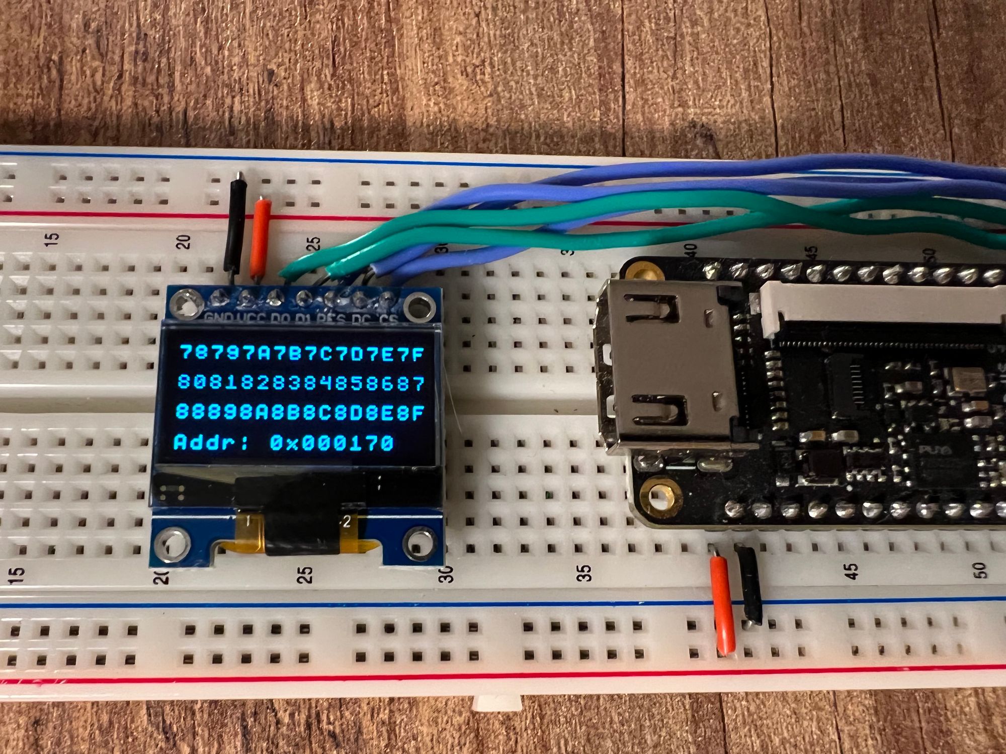
openFPGALoader -b tangnano9k --external-flash numbers.binAfter programming the flash, you should now see the first 32 bytes displayed on screen like the following:
The final step in our project is the navigation part.
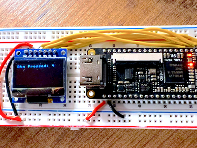
Navigating the Flash
We have already passed in our buttons into the flashNavigator module, so all we really need to do is let our buttons control which address we are reading, this can be done with two small changes to the flashNavigator.
The main change is to the done state:
STATE_DONE: begin
    dataReady <= 1;
    flashCs <= 1;
    dataInBuffer <= dataIn;
    counter <= STARTUP_WAIT;
    if (btn1 == 0) begin
        readAddress <= readAddress + 24;
        state <= STATE_INIT_POWER;
    end
    else if (btn2 == 0) begin
        readAddress <= readAddress - 24;
        state <= STATE_INIT_POWER;
    end
end
The first parts are exactly the same, but we add here two if statements. The first checks if the first button is pressed (active low buttons), if it is pressed we increment the read address by 24 and go back to the init state to restart the read process at the new address. The other button's if statement is very similar except we will decrement the readAddress allowing us to move in both directions.
We also need to change the STATE_INIT_POWER state to include a debounce on the buttons so that the loading will only happen on the release of the button so it doesn't scroll hundreds of times a second in a single button press.
STATE_INIT_POWER: begin
    if (counter > STARTUP_WAIT && btn1 == 1 && btn2 == 1) begin
        state <= STATE_LOAD_CMD_TO_SEND;
        counter <= 32'b0;
        dataReady <= 0;
        currentByteNum <= 0;
        currentByteOut <= 0;
    end
    else
        counter <= counter + 1;
end
The main change here is that we are not just waiting for the startup wait time we are also waiting for both button to be released before starting to load data from flash, again this is to debounce the button.
Now you might be asking, why are we advancing the counter by 24 bytes each time and not 32 like we are displaying ? The reason is I want to only display data on the top 3 lines and use the final line to display the current address.
Displaying the Current Address
We have a 24 bit address if we wanted to display it in HEX format we would need 6 hex characters. We could create 6 registers and 6 toHex modules one for each of the characters of the address manually, but verilog has a feature for situations like this where we can "generate" repetitive code in a sort of for loop:
genvar i;
generate
    for (i = 0; i < 6; i = i + 1) begin: addr
        wire [7:0] hexChar;
        toHex hexConv(
            clk,
            readAddress[{i, 2'b0}+:4],
            hexChar
        );
    end
endgenerate
We start by creating a special kind of variable called a genvar which is like a regular variable just only used in generate blocks. The generate block is sort of like a pre-processor where this block will be expanded and flattened into all the underlying modules it creates in the loop.
In our loop we are iterating 6 times, each time creating an 8 bit wire to reference the ASCII output from the hex conversion, and then we send the appropriate bits from readAddress to the conversion module.
You can also see on the line with the for loop we end the line with a colon (:) and a word addr this word is the name we are giving this block. We can name the block whatever we like just like other variables and it gives us a way to reference the variables instantiated inside. So for example if we want to access hexChar from the third iteration we can write addr[2].hexChar to reference it.
We can then change the always block to output a special address line on the 4th row:
always @(posedge clk) begin
    chosenByte <= dataInBuffer[(byteDisplayNumber << 3)+:8];
    if (charAddress[5:4] == 2'b11) begin
        case (charAddress[3:0])
            0: charOutput <= "A";
            1: charOutput <= "d";
            2: charOutput <= "d";
            3: charOutput <= "r";
            4: charOutput <= ":";
            6: charOutput <= "0";
            7: charOutput <= "x";
            8: charOutput <= addr[5].hexChar;
            9: charOutput <= addr[4].hexChar;
            10: charOutput <= addr[3].hexChar;
            11: charOutput <= addr[2].hexChar;
            12: charOutput <= addr[1].hexChar;
            13: charOutput <= addr[0].hexChar;
            15: charOutput <= dataReady ? " " : "L";
            default: charOutput <= " ";
        endcase
    end
    else
        charOutput <= hexCharOutput;
end
The first line stayed the same, then we check if we are on the 4th line or not. If so we output specific characters for each of the 16 characters in this row to spell out "Addr: 0x<addr>". We also added an "L" in the last position while loading, not that you will really be able to see it as it is super fast.
Running again you should see a working flash navigator where using the buttons we can see all 256 bytes we programmed into memory along with the address at the bottom of the screen.
Conclusion
In this article we explored the on-board flash IC and wrote a module allowing us to read data we programmed onto it. The project still has its flaws, like the address will underflow to FFFFFF which is not a valid address as with 4MB we only have up to 3FFFFF. But to not make a long article even longer we will leave it here for now.
This can also be extended as a personal exercise to change the project into a flash ASCII viewer loading and displaying 48 bytes of ASCII data besides the address row.
I would like to thank you for reading, hope you enjoyed, as always the code can be found on github here.
If you have any questions or comments feel free reach out by leaving a comment down below or on twitter @LushayLabs.
Also if you would like to purchase any of the components used in this series and support the site you can visit our store here.