
Up until now we have been dealing with all our procedural tasks by creating state machines that would advance step by step through a process. This is great for simpler tasks, but for more complex tasks it can grow out of hand quickly if proper care isn't made to craft the correct building blocks.
Think about explaining a simple circuit like a 4-bit adder, if your building blocks include a full-adder then it can be explained as 4 full adders chained together. Take the same circuit except your building block is logic gates it now requires 20 logic gates to create the 4-bit adder, and if we go down a layer to transistors we will have 40-50 transistors in our diagram.
The same idea is true with procedural tasks, if you have the right "building blocks" or sub-tasks, then composing the process because both easier, cleaner and can eliminate repetition or wasted resources.
In this article we will go through this process while integrating the ADS1115 ADC with the Tang Nano 9K over I2C, this will both add two new capabilities to our toolbelt (I2C & ADC) as well as a methodology which can be used to tackle even larger projects.
The I2C Protocol
I2C communicates over two wires, one wire is for data and one wire is for a clock. Unlike SPI, where you have a seperate data wire for each direction, in I2C both wires are bidirectional. Another difference is that with SPI if you want to connect multiple peripherals over the same wires you need to add an extra "chip select" or enable pin to select which device the controller is currently communicating with.
The I2C protocol has addressing built into the protocol, so you can connect multiple devices without requiring more IO from the controller. The standard address size for I2C is 7-bit allowing for potentially 128 different addresses (some addresses are reserved but theoretically) and there is also a 10-bit mode (which we won't get into) that would allow up to 1024 for each 2 IO pins.
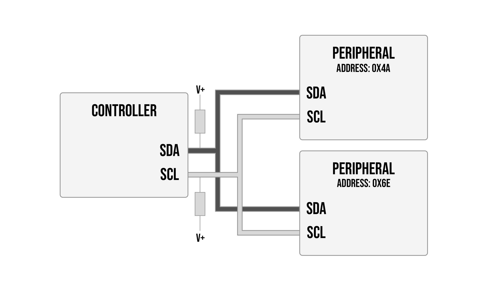
The way the communication works at the physical layer is that each line is pulled high through a resistor and any of the devices can pull the line low. The devices cannot see who pulled the line low just if the line is high or low, so the protocol relies on coordination and addressing to know who is sending / receiving data.
The controller is always in charge of driving the clock (even when a peripheral is sending data), and data is changed when the clock is low and read when the clock goes high. Changing the data line while the clock is high has a special meaning in I2C and is used to indicate the start / end of a transaction (communication).
Pulling the data line from high to low while the clock is high signifies a start of transmission and pulling the data from low to high while the clock is high signifies an end of transmission.
Transactions with I2C can be multiple bytes long, but after each byte is sent the receiving end (either controller or peripheral) acknowledges the byte by sending a zero on the data line.
So a typical transaction looks like the following:
The controller will send the start of transaction event (again by pulling the data low while clock is high), it will then send the 7 address bits MSB first, the last bit in the first byte is a bit to signify if the controller wants to read data from the addressed device or write data to the addressed device. A value of one is to read data from the device and a value of zero is to write.
The peripheral will then ack by sending a zero over the data line, and then the transaction will continue with the next byte being sent over the data line. In the case where the controller is reading the next byte will be sent by the peripheral and the controller will send the ACK and if the controller is writing to the peripheral then the controller will send this data and the peripheral will ACK.
No matter which device is controlling the data line (controller or peripheral), the clock line is always powered by the controller.
The data sending can be repeated multiple times to send multiple bytes in the same transaction, just like above after each byte the other side ACKS. Once all bytes of a transaction are sent the controller sends the "end of transmission" event, by pulling the data line high while the clock is high ending the transaction between the two devices.
To implement this the controller needs to read the clock line on each bit and make sure the clock went high when it set the clock high to make sure a peripheral isnt pulling it low
With an overview of the I2C protocol we can now dive into the datasheet for the ADC we will be using and start exploring how to interface with it.
The ADS1115
The ADS1115 is a 4-channel 16-bit ADC, this means you can connect up to 4 analog signals to it which it can mux between and it converts a chosen analog value into a 16-bit digital value.
Let's take a look at the datasheet to get more information on how to drive it.
On the first page we get a nice simplified block diagram:
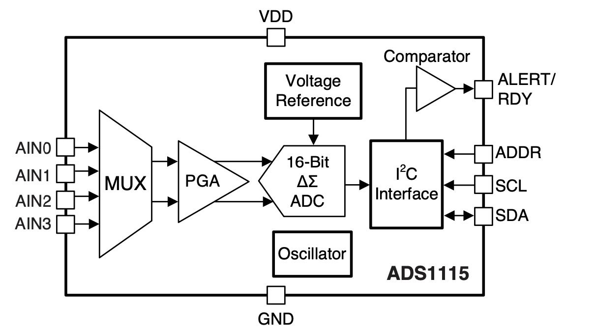
Here you can see the 4 analog inputs go through a mux and two lines go from the mux into the programmable gain amplifier. The reason there are two lines coming out of the mux is because you can use the ADS1115 to measure differential pairs, we will only be using the ADC to measure positive values so the mux will connect the other wire to ground.
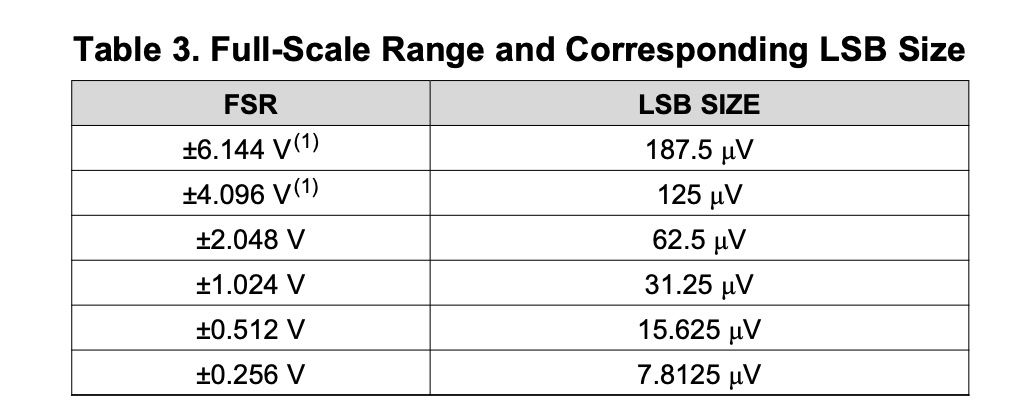
The programmable gain filter then remaps our input value to a predefined FSR, so if you are using low voltage for example max 2 volts you can program that in and then you will get the full 16-bits of precision for the range -2 to +2 volts meaning each increment would represent around 0.061 mv (4v range / 216) whereas if you set the range to +- 6v the precision of each increment would be 0.183mv (12v range / 216). So setting the PGA up as close to your real value range will give you the most accuracy.
The remapped value gets passed to the internal ADC which is then stored in a conversion register for the I2C interface to output. The Alert pin can be used to recieve a notification when the conversion is done / meets a threshold. We won't be using it as you can check the status over the I2C interface so we will get the info there.
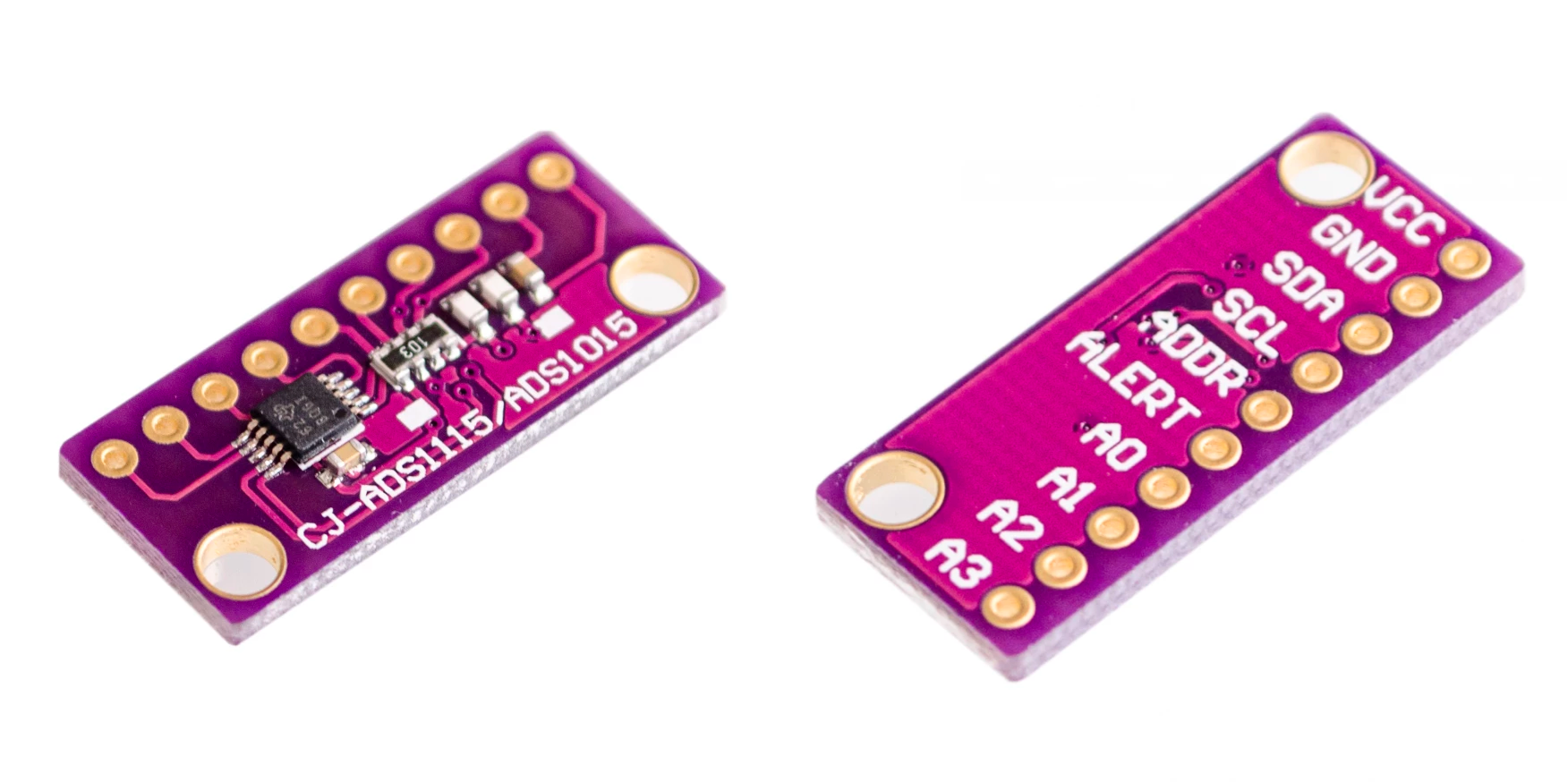
The ADDR pin of the I2C interface is used to setup the address, like mentioned above each I2C peripheral requires an address so that the controller can select it for communication. This pin, depending on how you connect it will set it's I2C address. Here is the table for the different options:
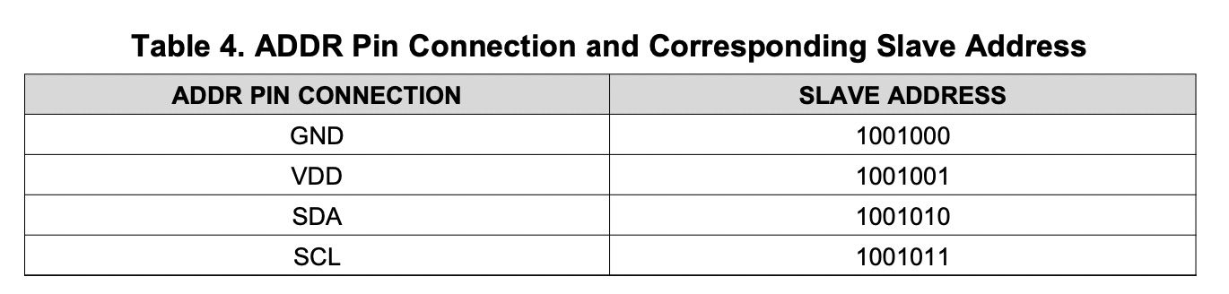
We will be connecting it to VDD so the address we will need to request is 1001000 in binary or 0x73 in hex. (Worth noting there is special care that needs to be taken if connecting the address pin to SDA so refer to the datasheet if that option is chosen).
The ADC has 4 main internal registers which we use to set up, control and read the conversion values from. The registers are:
- Conversion Register
- Config Register
- Low Threshold Register
- High Threshold Register
The first register stores the latest conversion results. The second register is where we setup the ADC, as-well as where we request it to perform a new conversion. The last two registers are used if you want to setup the internal comparator to signal when it is in a certain range. We won't be using the comparator so we mainly need to focus on the first two registers.
The conversion register is read only and the config register we need to read and write. We need to write the initial config and to trigger a new conversion, and we need to read from it to check when a conversion is ready.
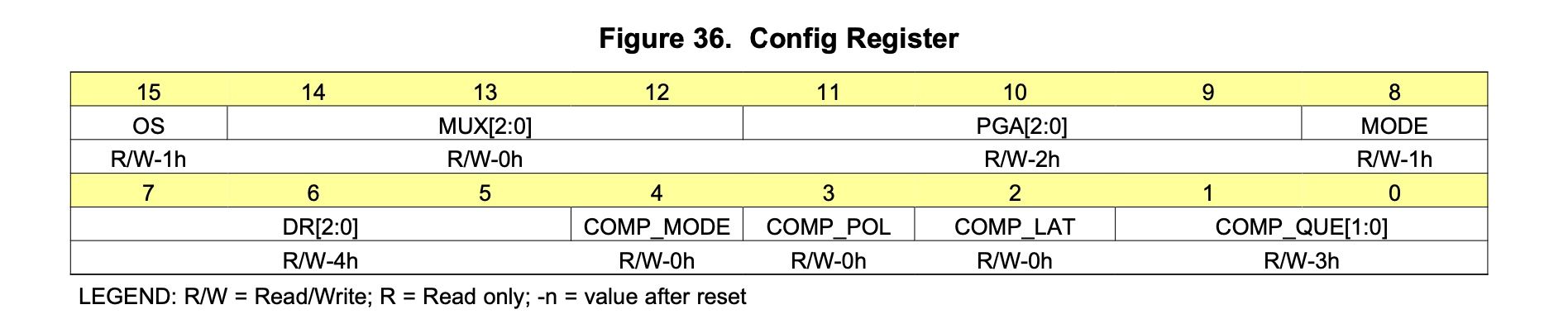
The first bit OS triggers a new conversion when set, and when reading the conversion register it will be a 1 if the ADC is idle (meaning the conversion is done). Next we have 3 bits which control the MUX meaning which analog channel is currently connected to the internal ADC. The next 3 bits we talked about control the programmable gain amplifier and the MODE bit sets whether we are in continuous conversion mode or single conversion mode. Like the names suggest in continuous mode the ADC will start a new conversion once it completes the current conversion, and in single shot mode each time you trigger the conversion it will perform only 1 conversion.
The Second byte in the config register is for the comparator, which again we will not be using so we will leave the default values for them.
We will be using the ADC in single-shot mode, which means the general game plan is we need to write a 1 in the OS bit to start a conversion while setting the MUX to the correct channel, we then need to wait until the conversion is done, which we will see by OS being high while being read. Once the value is ready we need to read the digital value from the conversion register.
With the high level plan out of the way, how do we actually communicate these instructions to the ADS1115 ?
The Communication
We basically have two types of commands we can issue, a write command which has the following interface:
<Address><W> <Register Select> <Optional Data 16-bit> By sending the I2C address along with a zero for the read/write bit, it tells the ADC you want to write to a register, the first byte sent after this is the destination register from one of the 4 registers listed above. Once you select a register you can optionally write a value to that register by writing another 2 bytes of data.
If you don't send data, then the write command simply changes the currently selected register, which is needed for example if you want to select the conversion register in-order to read from it.
In-order to read a register you need to again make sure you already selected the corrected register by issuing a write command and then you send a read command with the following interface:
<Address><R> <16-bit data>Now these two interfaces are a bit simplified as for I2C you need to send a start / end transaction event, and there is also an ACK after every byte, so let's take a look at the full process for each of these commands from the datasheet:
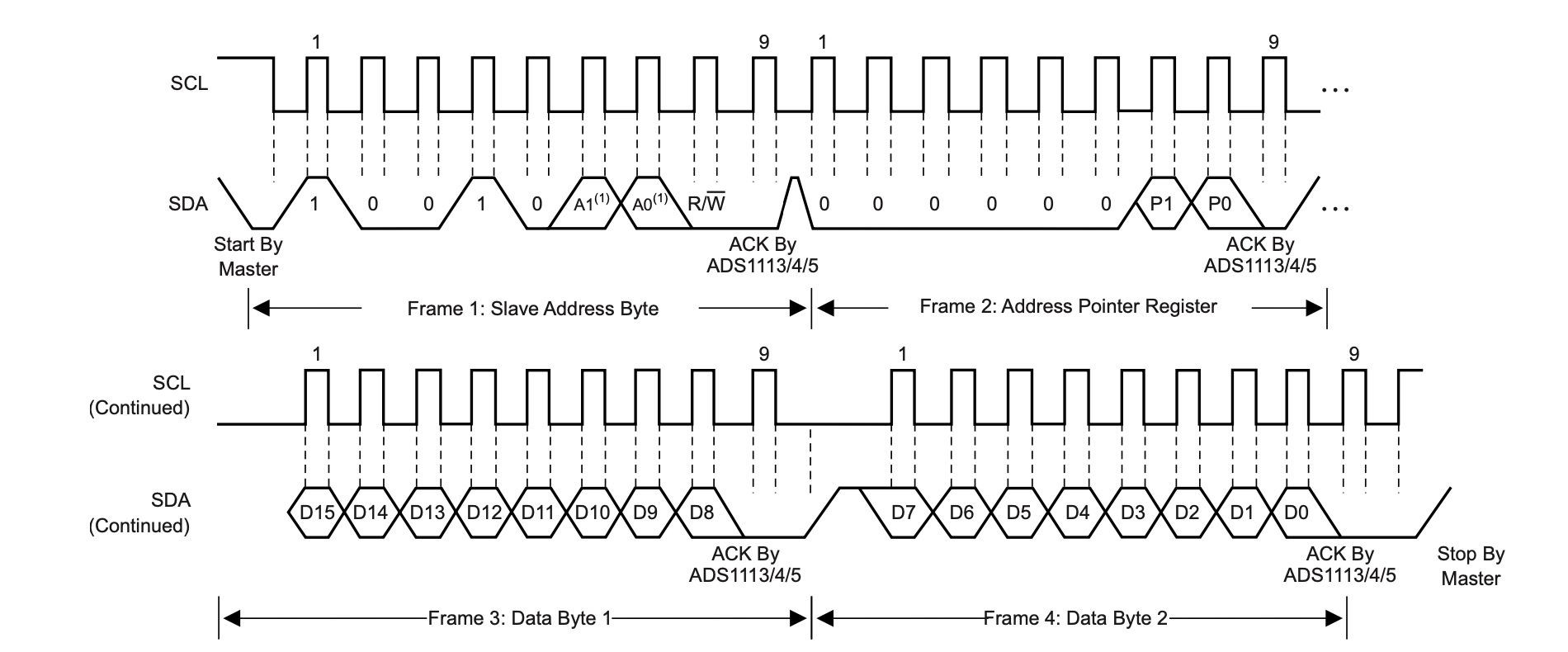
This diagram shows a complete write sequence. We start the transmission by pulling SDA low while SCL is high. We then send the address of the peripheral along with a zero for the R/W bit followed by an ACK from the ADC. The next byte selects one of the 4 main registers again it is followed by an ACK. The final two bytes send the data, most significant bit and most significant byte first and each of the two bytes has its own ACK. Finally we send an end of transmission by pulling SDA high while SCL is high.
The process for reading is as follows:
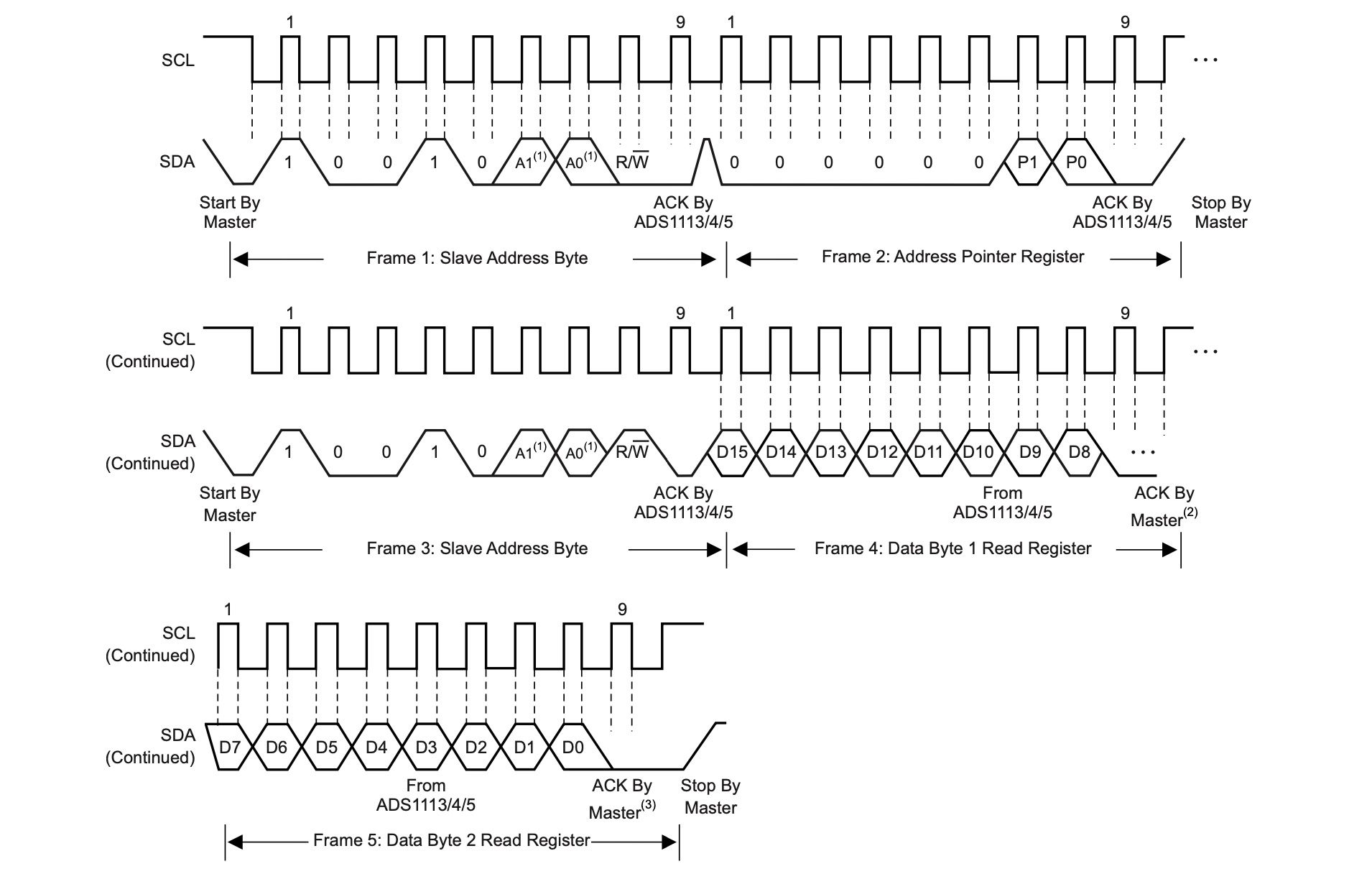
The first two bytes are like above, because they are essentially a write command without data to select the correct register, you can see after these first to bytes there is an end of transmission (Stop signal) separating it from the read. Once the register is selected we issue a new I2C command with a new start of transmission, this time with a one for the R/W bit to signify we want to read data, followed by us clocking two bytes worth of clock signals (plus ACK bits) to receive the full 16 bits of the selected register.
Now these two flows are just how to write and read registers, in-order to perform a full conversion we will need to read and write multiple registers. The entire flow is:
- Write to config register to setup general configuration and start conversion
- Read config register until you see the conversion is complete
- Read conversion register.
Creating a state machine for this whole process where you directly control SDA and SCL would result in a very large and complex state machine. Even within a single sub-task, for example reading a register, we have 5 bytes, some of which we are sending, some we are receiving, We need to send a start and stop event in the middle unlike with the write command here we don't want to continue writing data, etc.. It's not that it can't be done, it's just like the example of drawing a circuit diagram with only transistors it can be done, but is unnecessarily complex.
Let's us try and break up the two commands we saw above into reusable components.
Sub Tasks
Now there are multiple ways of splitting a large process into sub-tasks, and multiple layers of granularity that you can use. One method is to look for repetition, if we take a look at our end process, we need to write to 1 register and read from two others.
If we had a sub-task for read register and write register we could compose our main conversion flow pretty easily. The problem with this idea is like mentioned each of these tasks on their own is already pretty large. So let's go down a level and take a look if we can split the read / write register commands themselves into smaller composable parts.
For example let's break up the two flows into the following sub-tasks
- Start a TX
- Stop a TX
- Read a byte + send ack
- Write a byte + receive ack
Looking at the write register example with this split:
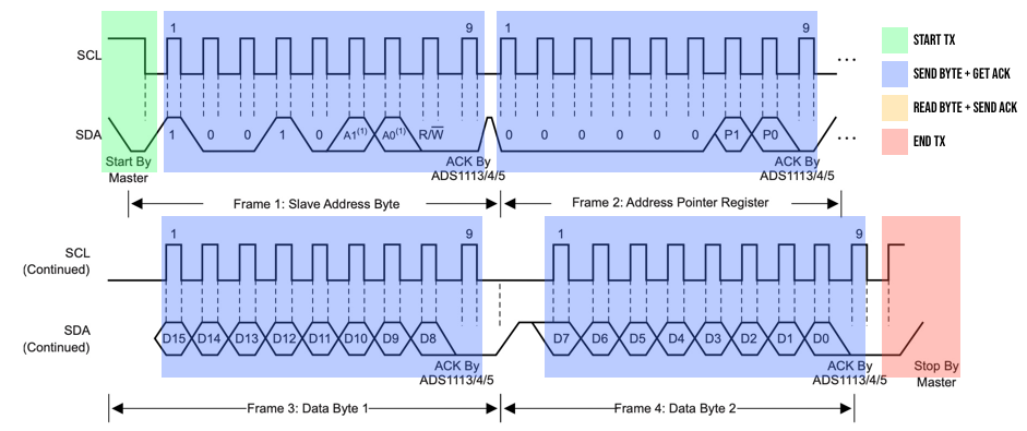
We can see it can easily be defined as 6 sub-commands:
1. Start TX
2. Send (Address + R/W) then get Ack
3. Send Register index then get ack
4. Send top byte then get ack
5. Send bottom byte then get ack
6. End TX
If sub-tasks were functions in a higher level programming language we would have something like the following:
start_i2c()
send_byte((address << 1) + readWriteBit)
send_byte(registerIndex)
send_byte(topByte)
send_byte(bottomByte)
stop_i2c()
And if we take a look at reading a register we have something like the following:
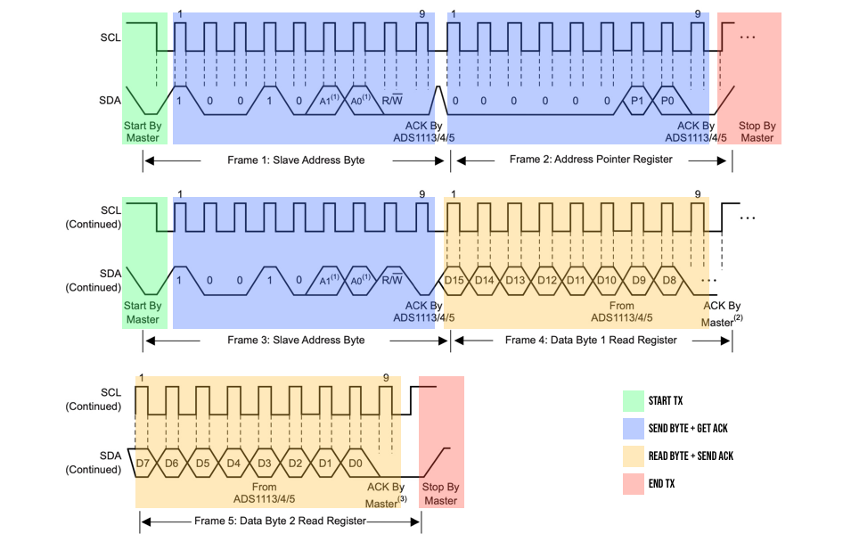
Here we can first of all split this into two main tasks:
- Point to the correct register
- Read the register
And each of these tasks can be split into our 4 sub-tasks like with the write example. Using this split, we have a very manageable sub-task layer with only 4 operations each of which being pretty straightforward to implement as they are limited to a single byte and then we can easily compose them into each of the operations we need to perform a conversion.
Let us restate the conversion process now from start to finish using our 4 components
// Task 0 Setup Conversion
 - 0 start_i2c()
 - 1 send_byte({address, w})
 - 2 send_byte(select_config_register)
 - 3 send_byte(config_with_channel_upper)
 - 4 send_byte(config_with_channel_lower)
 - 5 stop_i2c()

// Task 1 Check if Ready
 - 0 wait x amount of time
 - 1 start_i2c()
 - 2 send_byte({address, r})
 - 3 read_byte() // reading config upper byte
 - 4 store 1st byte + read_byte() // reading config lower byte
 - 5 stop_i2c()

// Task 2 Switch Back to Conversion Register
 - 0 delay some time
 - 1 start_i2c()
 - 2 write_byte({address, w})
 - 3 write_byte(select_conversion_register)
 - 4 stop_i2c()

// #3 Read Value
 - 0 start_i2c()
 - 1 write_byte({address, r})
 - 2 read_byte() // reading conversion register upper
 - 3 store 1st byte + read_byte() // reading conversion register lower
 - 4 store 2nd read byte
 - 5 stop_i2c()
By abstracting the physical I2C stuff into its own layer we are able to easily copy the diagrams from the ADC datasheet we color coded in-order to represent the full flow.
This change lowered the total states required to 19, but we can do even better. Taking a look at the states listed above we can see multiple duplicates for example:
Task 0 - Subtask 0
Task 1 - Subtask 1
Task 2 - Subtask 1
Task 3 - Subtask 0
Are all start_i2c and we also have 4 stop_i2c steps, reading bytes is also the same for both tasks 1 and 3, etc.. Going through the list we can narrow down the number of unique states we need to create using our building blocks to only 11. This means we can create these 11 micro procedures along with the 4 sub-tasks we used as our building block for a total of 15 states.
So with a plan of attack, let's get into the implementation.
The Implementation
In a new folder in VSCode let's start off by creating our building blocks by implementing the I2C physical layer. To do this let's create a new file called i2c.v with the following module:
`default_nettype none

module i2c (
    input clk,
    input sdaIn,
    output reg sdaOutReg = 1,
    output reg isSending = 0,
    output reg scl = 1,
    input [1:0] instruction,
    input enable,
    input [7:0] byteToSend,
    output reg [7:0] byteReceived = 0,
    output reg complete
);
endmodule
We have a bunch of inputs and outputs so let's go through them 1 at a time. We start with the main clock signal, then we have three registers for the I2C SDA line. I2C - being a bidirectional interface on a single line - relies on each side both being able to read and write to the same wire.
This is accomplished by using tristate logic and the special inout keyword to signify the wire can be used as both an input and an output. FPGAs have limited support for tristate logic but the IO pins have their own tri-state registers, because of this we will separate our module from the tristate logic giving the pnr the flexibility to place each where it fits best. So in our module we use two separate wires for each direction and an extra wire to say which if we are currently inputting data or outputting.
Basically in the top module we can do something like the following to control the tristate io pin:
module top(
 inout i2cSDA
);
    assign i2cSDA = isSending ? sdaOutReg : 1'bz;
endmodule
So if we are currently sending over the SDA line then connect the pin to the output register for SDA otherwise if we are currently reading, then sets the wire to high-impedance state (using the special z bit literal) which means no value is driven on the line and we will be able to read the outside value making it an input.
It's worth noting that I2C uses an open-drain configuration, which means the line itself is pulled high externally through a pull-up resistor and each side can only pull the line low. The main difference between this configuration and a standard configuration (like in the code example above) is that in an open-drain configuration if either side pulls the line low, the line is definitely low and in a standard situation if 1 side pulls the line low and the either side high the line will be high.
This ability for either side to force the line low allows for clock stretching, making the receiver of data "pause" the transmission if it needs more time to process something.
The implementation for an open-drain style connection we change the assign to something like the following:
assign i2cSDA = (isSending & ~sdaOutReg) ? 1'b0 : 1'bz;So if we are sending data and the bit we want to send is zero, then we pull the line low, if we are sending a one or inputting data we stop driving the line and rely on the external pullup to set the line high, but we will get to this code when we write the top module.
It is also worth noting that in the constraints file you can theoretically set the pin mode to open drain which will handle this automatically.
Back to our i2c module's inputs, we next have an output wire for SCL here we are not using a tristate buffer and simply an output wire since we don't need to support clock-stretching in our use-case.
Next we receive a 2 bit instruction, this will represent which of the 4 sub-tasks we currently would like to perform from:
- Start I2C
- Stop I2C
- Read Byte + Ack
- Write Byte + Ack
After the instruction we have an enable pin, for an outside module to trigger the module to perform the current instruction chosen (as opposed to being idle). The next is an 8-bit value to send (in the even of a write byte instruction) and the byteReceived buffer will be used to output a byte when the read byte instruction was used
The final output is a wire so that the i2c module can let the module using it know that the instruction is complete and it can move onto the next instruction.
Now let's create our states for the module's state machine:
localparam INST_START_TX = 0;
localparam INST_STOP_TX = 1;
localparam INST_READ_BYTE = 2;
localparam INST_WRITE_BYTE = 3;
localparam STATE_IDLE = 4;
localparam STATE_DONE = 5;
localparam STATE_SEND_ACK = 6;
localparam STATE_RCV_ACK = 7;
We start with our 4 instructions so that their index matches what will be in the instruction input. After the instructions we have an idle state which is the default state when no-one is communicating over I2C. The done state is for letting the external module who executed an I2C instruction that the instruction is complete.
The last two states are continuations of the read and write instructions, when reading we need to send an ACK and we writing we need to receive an ACK.
Next we will need 3 registers:
reg [6:0] clockDivider = 0;

reg [2:0] state = STATE_IDLE;
reg [2:0] bitToSend = 0;
By default the ADS1115 supports up to 400 kHz communication, there is also a high-speed 3.4 MHz mode but you have to enable it. We will be using the standard mode so we will need to divide our 27MHz clock down to something under 400 kHz.
If we divide the clock by 128 (or 2^7) then we get a little over 200 kHz and its a power of 2 making it easier to work with. So because of this we will create a 7-bit register which will count clock cycles.
Next we have a register to hold the current state, we will default to the idle state. Lastly we have a register to count which bit of a byte we are on, some of the states like sending or receiving are based around a byte of data, so we will use bitToSend to remember which bit we are on.
Next we need an always block for our state machine:
always @(posedge clk) begin
    case (state)
    	// states here
    endcase
end
The I2C States
The first state we will implement is the idle state, here we just wait until the enable pin is pulled high in which case we will start performing the operation passed in:
STATE_IDLE: begin
    if (enable) begin
        complete <= 0;
        clockDivider <= 0;
        bitToSend <= 0;
        state <= {1'b0,instruction};
    end
end
We set complete low since we are starting a new operation, we reset our two counter registers and we jump to the state matching the instruction number.
The next state is the I2C start condition which is when both clock and data lines are high and we pull the data line down before pulling the clock line down.
INST_START_TX: begin
    isSending <= 1;
    clockDivider <= clockDivider + 1;
    if (clockDivider[6:5] == 2'b00) begin
        scl <= 1;
        sdaOutReg <= 1;
    end else if (clockDivider[6:5] == 2'b01) begin
        sdaOutReg <= 0;
    end else if (clockDivider[6:5] == 2'b10) begin
        scl <= 0;
    end else if (clockDivider[6:5] == 2'b11) begin
        state <= STATE_DONE;
    end
end
We start by setting the isSending flag high to take control over SDA and we start counting clock cycles. We then divide the entire SCL clock time (~200 kHz) into 4 equal sections by looking only at the top two bits.
In the first section both lines are high, we then pull SDA low followed by pulling the clock line low. We wait one more period and then move to the done state.
We wait one more period before completing the instruction so that we stop in-between the low-clock pulse of SCL just like we blocked out in the image when above.
The next state / instruction is the stop condition state, it is exactly like the start just reversed:
INST_STOP_TX: begin
    isSending <= 1;
    clockDivider <= clockDivider + 1;
    if (clockDivider[6:5] == 2'b00) begin
        scl <= 0;
        sdaOutReg <= 0;
    end else if (clockDivider[6:5] == 2'b01) begin
        scl <= 1;
    end else if (clockDivider[6:5] == 2'b10) begin
        sdaOutReg <= 1;
    end else if (clockDivider[6:5] == 2'b11) begin
        state <= STATE_DONE;
    end
end
Both lines start off low, and we first pull the clock high and only after that SDA.
The next instruction is to read a byte of data:
INST_READ_BYTE: begin
    isSending <= 0;
    clockDivider <= clockDivider + 1;
    if (clockDivider[6:5] == 2'b00) begin
        scl <= 0;
    end else if (clockDivider[6:5] == 2'b01) begin
        scl <= 1;
    end else if (clockDivider == 7'b1000000) begin
        byteReceived <= {byteReceived[6:0], sdaIn ? 1'b1 : 1'b0};
    end else if (clockDivider == 7'b1111111) begin
        bitToSend <= bitToSend + 1;
        if (bitToSend == 3'b111) begin
            state <= STATE_SEND_ACK;
        end
    end else if (clockDivider[6:5] == 2'b11) begin
        scl <= 0;
    end
end
This is the first state where we are setting not controlling the SDA line and we will instead be using it as an input. Next we have the first quarter cycle with the clock low, and in the second quarter we set the clock high.
Taking a look at the 4 quarters of our SCL cycle:
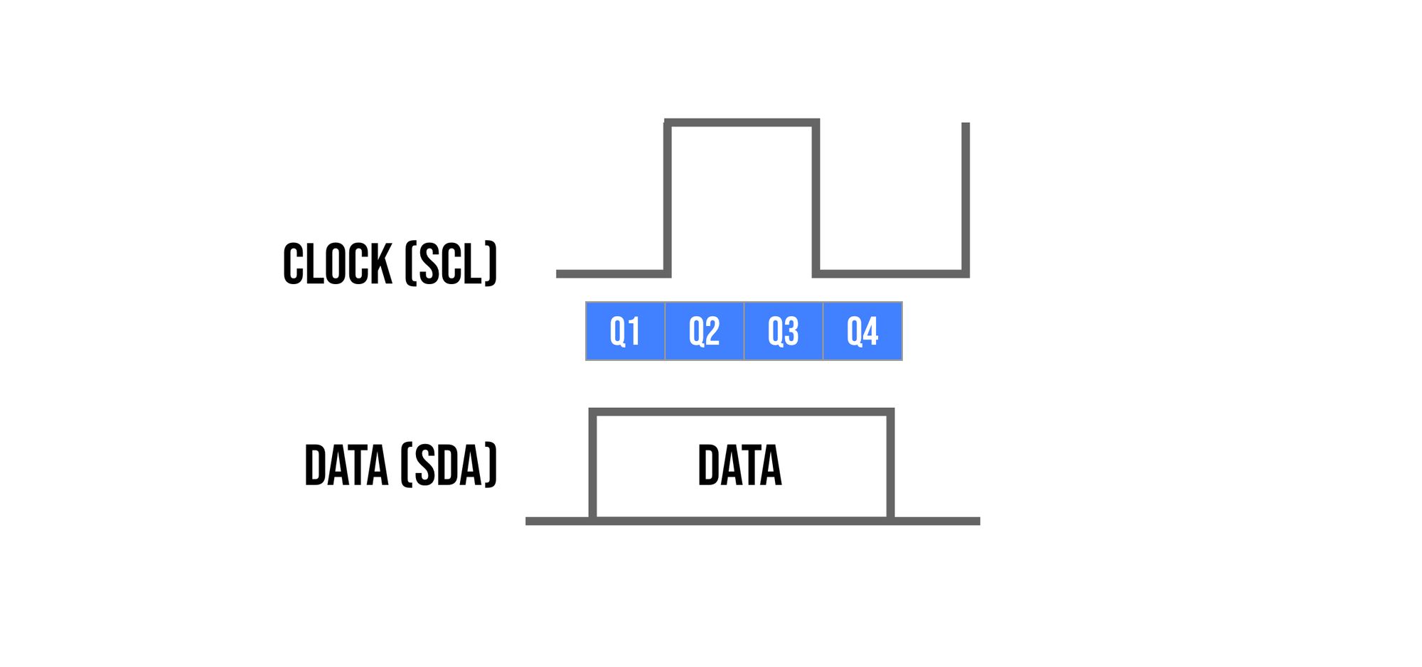
We see that we want to read when Q3 starts exactly in the middle of the clock cycle, so that is the next if condition when clockDivider equals 7'b1000000. Another way of looking at this value is that the top two bits are the quarter index and the rest are the sub-quarter counter. So we want quarter 10 which is 2 in decimal which represents the 3rd quarter (index starts at 0) and if all the other bits are zero then we are at the beginning of this quarter.
When we reach this point we shift the value of SDA into byteReceived and shift all the other bits up meaning the first bit we receive will be the most significant bit.
Next we have another special "time" which is when clockDivider equals 7'b1111111 which means quarter index 3 (or Q4) and all the other bits are 1 so at the end of Q4.
At this stage in time, we have completed a single bit, here we check if we are already on the last bit, if so we move onto the ACK, otherwise we just continue which will cause clockDivider to overflow back to zero starting the cycle over for the next bit.
The last condition is what to do in the rest of Q4 and that is to pull the clock low.
To send the ACK we just need to hold SDA low and pulse 1 SCL clock cycle:
STATE_SEND_ACK: begin
    isSending <= 1;
    sdaOutReg <= 0;
    clockDivider <= clockDivider + 1;
    if (clockDivider[6:5] == 2'b01) begin
        scl <= 1;
    end else if (clockDivider == 7'b1111111) begin
        state <= STATE_DONE;
    end else if (clockDivider[6:5] == 2'b11) begin
        scl <= 0;
    end
end
While sending the ACK we retake control over SDA by setting isSending high, we also set sdaOutReg low to send the low ACK signal. The rest is a simple SCL clock pulse, going high at the start of Q2 and going high at the start of Q4.
With the reading of a byte complete, writing a byte is pretty much at least in structure:
INST_WRITE_BYTE: begin
    isSending <= 1;
    clockDivider <= clockDivider + 1;
    sdaOutReg <= byteToSend[3'd7-bitToSend] ? 1'b1 : 1'b0;

    if (clockDivider[6:5] == 2'b00) begin
        scl <= 0;
    end else if (clockDivider[6:5] == 2'b01) begin
        scl <= 1;
    end else if (clockDivider == 7'b1111111) begin
        bitToSend <= bitToSend + 1;
        if (bitToSend == 3'b111) begin
            state <= STATE_RCV_ACK;
        end
    end else if (clockDivider[6:5] == 2'b11) begin
        scl <= 0;
    end
end
We set sdaOutReg to the corresponding bit we currently want to send starting with bit index 7 or the most significant bit. The rest is pretty much just to clock an SCL clock cycle and we have the condition for the end of Q4 to see if we have completed all 8 bits.
STATE_RCV_ACK: begin
    isSending <= 0;
    clockDivider <= clockDivider + 1;

    if (clockDivider[6:5] == 2'b01) begin
        scl <= 1;
    end else if (clockDivider == 7'b1111111) begin
        state <= STATE_DONE;
    end else if (clockDivider[6:5] == 2'b11) begin
        scl <= 0;
    end
    // else if (clockDivider == 7'b1000000) begin
    //     sdaIn should be 0
    // end
end
While receiving the ack we need to clock out an SCL clock pulse and theoretically during the high part of the clock pulse we should see that the peripheral pulled the SDA line low. We won't really be checking it, which is why I left it as a comment since we won't really be handling that case so there is no point checking it. If you do want to handle it then you need to decide what happens if an error was detected, like for example sending an end condition over I2C and setting an error flag instead of complete to let the upper modules know their was an issue and retry or something.
The final state is the done state where we only let the external module know the I2C instruction is complete and we wait for them to acknowledge by releasing the enable input, this way we have two way validation.
STATE_DONE: begin
    complete <= 1;
    if (~enable)
        state <= STATE_IDLE;
end
With that we have our 4 I2C building blocks and we can move onto building the ADC module.
The ADC Module
To begin with let's create a new file called adc.v with the following module:
`default_nettype none

module adc #(
    parameter address = 7'd0
) (
    input clk,
    input [1:0] channel,
    output reg [15:0] outputData = 0,
    output reg dataReady = 1,
    input enable,
    output reg [1:0] instructionI2C = 0,
    output reg enableI2C = 0,
    output reg [7:0] byteToSendI2C = 0,
    input [7:0] byteReceivedI2C,
    input completeI2C
);

endmodule
We start off with a parameter for the peripheral address which we need to send with each I2C command. Next for inputs we have the clock, an input for which of the 4 ADC channels we want to read, a register for the 16-bit output data and 2 flags one for this module to say when it has data ready and one for the top module to request a conversion (enable).
The rest of the ports are the connections required to interface with the I2C module we created.
// setup config
reg [15:0] setupRegister = {
    1'b1, // Start Conversion
    3'b100, // Channel 0 Single ended
    3'b001, // FSR +- 4.096v
    1'b1, // Single shot mode
    3'b100, // 128 SPS
    1'b0, // Traditional Comparator
    1'b0, // Active low alert
    1'b0, // Non latching
    2'b11 // Disable comparator
};

localparam CONFIG_REGISTER = 8'b00000001;
localparam CONVERSION_REGISTER = 8'b00000000;
Next let's setup some things from the data sheet. The setup register holds the values we want to put in the config register. The only thing that needs to be changed here is the channel each time depending on which channel was requested.
The last two local parameters are what needs to be send in order to choose the respective register after sending an I2C write command.
Now we can define our sub tasks:
localparam TASK_SETUP = 0;
localparam TASK_CHECK_DONE = 1;
localparam TASK_CHANGE_REG = 2;
localparam TASK_READ_VALUE = 3;

localparam INST_START_TX = 0;
localparam INST_STOP_TX = 1;
localparam INST_READ_BYTE = 2;
localparam INST_WRITE_BYTE = 3;
The 1st 4 are the sub tasks for the ADC module and the last 4 are the instructions we can send to the I2C module. The plan is to implement each of our 4 ADC sub tasks using the I2C instructions we created as follows:
| Stage | Step | Description |
|---|---|---|
| TASK_SETUP | 0 | Start I2C |
| TASK_SETUP | 1 | Send Byte {address, w} |
| TASK_SETUP | 2 | Send Byte to select config register |
| TASK_SETUP | 3 | Send Byte with config's upper byte |
| TASK_SETUP | 4 | Send Byte with config's lower byte |
| TASK_SETUP | 5 | Stop I2C |
| TASK_CHECK_DONE | 0 | Delay some time |
| TASK_CHECK_DONE | 1 | Start I2C |
| TASK_CHECK_DONE | 2 | Send Byte {address, r} |
| TASK_CHECK_DONE | 3 | Read Byte |
| TASK_CHECK_DONE | 4 | Store 1st read byte, Read Byte |
| TASK_CHECK_DONE | 5 | Stop I2C |
| TASK_CHANGE_REG | 0 | Verify conversion is ready |
| TASK_CHANGE_REG | 1 | Start I2C |
| TASK_CHANGE_REG | 2 | Send Byte {address, w} |
| TASK_CHANGE_REG | 3 | Send Byte to change to conversion register |
| TASK_CHANGE_REG | 4 | Stop I2C |
| TASK_READ_VALUE | 0 | Start I2C |
| TASK_READ_VALUE | 1 | Send Byte {address, r} |
| TASK_READ_VALUE | 2 | Read Byte |
| TASK_READ_VALUE | 3 | Store 1st read byte, Read Byte |
| TASK_READ_VALUE | 4 | Store 2nd read byte |
| TASK_READ_VALUE | 5 | Stop I2C |
The way we will do this is like in a sequential processor. When a conversion is requested we will start processing each of these in order, each time performing an action and incrementing the task counter through these stages and steps.
localparam STATE_IDLE = 0;
localparam STATE_RUN_TASK = 1;
localparam STATE_WAIT_FOR_I2C = 2;
localparam STATE_INC_SUB_TASK = 3;
localparam STATE_DONE = 4;
localparam STATE_DELAY = 5;
Idle and done states are like we saw in the I2C module, one is the default idle state and the other is to send the done flag up to the top module.
Our core flow will be:
- Run task step by running an I2C instruction
- Wait for I2C to say the instruction is done
- Increment task counter to move to next task
The final delay state is for waiting between starting a conversion and for the result to be ready.
Our state machine will need the following registers:
reg [1:0] taskIndex = 0;
reg [2:0] subTaskIndex = 0;
reg [4:0] state = STATE_IDLE;
reg [7:0] counter = 0;
reg processStarted = 0;
task and subtask index hold where we are in our process table above, the state is the current state in our state machine the counter will be used in the delay and the processStarted flag bit will be used when waiting for the I2C instruction to finish.
The ADC State Machine
We basically have two state machines in one here, we have the macro state machine or the outer one which handles our core loop and we have a micro state machine which will be going through all the tasks and subtasks from our table required to perform a full conversion.
To start we can create the outer state machine:
always @(posedge clk) begin
    case (state)
        // outer states here
    endcase
end
The first state here is the idle state:
STATE_IDLE: begin
    if (enable) begin
        state <= STATE_RUN_TASK;
        taskIndex <= 0;
        subTaskIndex <= 0;
        dataReady <= 0;
        counter <= 0;
    end
end
We wait for the enable signal which advances us to the state with our internal state machine. Other then that we reset all our registers.
The run task is a bit long as it holds our complete internal state machine but I will add the whole thing so as not to confuse which states are part of the outer and which are part of the inner state machine:
STATE_RUN_TASK: begin
    case ({taskIndex,subTaskIndex})
        {TASK_SETUP,3'd0},
        {TASK_CHECK_DONE,3'd1},
        {TASK_CHANGE_REG,3'd1},
        {TASK_READ_VALUE,3'd0}: begin
            instructionI2C <= INST_START_TX;
            enableI2C <= 1;
            state <= STATE_WAIT_FOR_I2C;
        end
        {TASK_SETUP,3'd1},
        {TASK_CHANGE_REG,3'd2},
        {TASK_CHECK_DONE,3'd2},
        {TASK_READ_VALUE,3'd1}: begin
            instructionI2C <= INST_WRITE_BYTE;
            byteToSendI2C <= {
                address,
                (taskIndex == TASK_CHECK_DONE || taskIndex == TASK_READ_VALUE) ? 1'b1 : 1'b0
            };
            enableI2C <= 1;
            state <= STATE_WAIT_FOR_I2C;
        end
        {TASK_SETUP,3'd5},
        {TASK_CHECK_DONE,3'd5},
        {TASK_CHANGE_REG,3'd4},
        {TASK_READ_VALUE,3'd5}: begin
            instructionI2C <= INST_STOP_TX;
            enableI2C <= 1;
            state <= STATE_WAIT_FOR_I2C;
        end
        {TASK_SETUP,3'd2},
        {TASK_CHANGE_REG,3'd3}: begin
            instructionI2C <= INST_WRITE_BYTE;
            byteToSendI2C <= taskIndex == TASK_SETUP ?
                CONFIG_REGISTER : CONVERSION_REGISTER;
            enableI2C <= 1;
            state <= STATE_WAIT_FOR_I2C;
        end
        {TASK_SETUP,3'd3}: begin
            instructionI2C <= INST_WRITE_BYTE;
            byteToSendI2C <= {
                setupRegister[15] ? 1'b1 : 1'b0,
                1'b1, channel,
                setupRegister[11:8]
            };
            enableI2C <= 1;
            state <= STATE_WAIT_FOR_I2C;
        end
        {TASK_SETUP,3'd4}: begin
            instructionI2C <= INST_WRITE_BYTE;
            byteToSendI2C <= setupRegister[7:0];
            enableI2C <= 1;
            state <= STATE_WAIT_FOR_I2C;
        end
        {TASK_CHECK_DONE,3'd0}: begin
            state <= STATE_DELAY;
        end
        {TASK_CHECK_DONE,3'd3},
        {TASK_READ_VALUE,3'd2}: begin
            instructionI2C <= INST_READ_BYTE;
            enableI2C <= 1;
            state <= STATE_WAIT_FOR_I2C;
        end
        {TASK_CHECK_DONE,3'd4},
        {TASK_READ_VALUE,3'd3}: begin
            instructionI2C <= INST_READ_BYTE;
            outputData[15:8] <= byteReceivedI2C;
            enableI2C <= 1;
            state <= STATE_WAIT_FOR_I2C;
        end
        {TASK_CHANGE_REG,3'd0}: begin
            if (outputData[15])
                state <= STATE_INC_SUB_TASK;
            else begin
                subTaskIndex <= 0;
                taskIndex <= TASK_CHECK_DONE;
            end
        end
        {TASK_READ_VALUE,3'd4}: begin
            state <= STATE_INC_SUB_TASK;
            outputData[7:0] <= byteReceivedI2C;
        end
        default:
            state <= STATE_INC_SUB_TASK;
    endcase
end
It may be long, but each case is pretty simple. In-order to use the I2C building block we only need to set the instruction, enable the I2C module and wait for it to be done, we can also optionally set byteToSendI2C if we are writing a byte.
So you can see for example, there are 4 steps that we are supposed to send a start i2c instruction and the code looks like the following:
{TASK_SETUP,3'd0},
{TASK_CHECK_DONE,3'd1},
{TASK_CHANGE_REG,3'd1},
{TASK_READ_VALUE,3'd0}: begin
    instructionI2C <= INST_START_TX;
    enableI2C <= 1;
    state <= STATE_WAIT_FOR_I2C;
end
I won't go through all these tasks, but taking a look at the table above explains what each one is doing, and they are all in the same format as the above start task.
The next task in our macro state machine is the "wait for i2c" state:
STATE_WAIT_FOR_I2C: begin
    if (~processStarted && ~completeI2C)
        processStarted <= 1;
    else if (completeI2C && processStarted) begin
        state <= STATE_INC_SUB_TASK;
        processStarted <= 0;
        enableI2C <= 0;
    end
end
We start by waiting for the I2C to be in the middle of a conversion and then we wait for the I2C module to say it is complete. The reason we first wait for the I2C to be busy is so that we don't accidently read the previous commands complete signal as the new instructions complete signal.
The next state is for incrementing where we are in our micro process:
STATE_INC_SUB_TASK: begin
    state <= STATE_RUN_TASK;
    if (subTaskIndex == 3'd5) begin
        subTaskIndex <= 0;
        if (taskIndex == TASK_READ_VALUE) begin
            state <= STATE_DONE;
        end
        else
            taskIndex <= taskIndex + 1;
        end
    else
        subTaskIndex <= subTaskIndex + 1;
end
We saw that none of our stages has more then 5 sub-steps so if the sub-task index equals 5 we can move onto the next step otherwise we just increment the sub-task index.
Next we have a state to wait a bit before checking if the conversion results are ready:
STATE_DELAY: begin
    counter <= counter + 1;
    if (counter == 8'b11111111) begin
        state <= STATE_INC_SUB_TASK;
    end
end
He just count 256 clock cycles which at 27 Mhz is about 10 microseconds of delay.
Finally we have the done state which just sets the data ready flag high and waits for the enable input to go low as acknowledgement:
STATE_DONE: begin
    dataReady <= 1;
    if (~enable)
        state <= STATE_IDLE;
end
With that the ADC module is done, it's a bit long, but I think you can agree that each single sub task is very simple and by using the table containing the procedures it's easy to know what to do at each step.
Now this article is running a bit long, but I think it is worth us taking one last detour to create a testbench before we wrap up with a final test case.
Testing the ADC
To test we need to create a new testbench file, so let's create a file called adc_tb.v We can start off with some boilerplate:
module test();

reg clk = 0;

always
    #1  clk = ~clk;

initial begin
    #100000 $finish;
end


initial begin
    $dumpfile("adc.vcd");
    $dumpvars(0,test);
end
endmodule
This just sets up our clock signal and the VCD output. We also set the length of our test to 100000 time units (where each clock cycle is 2 time units).
Now we have to create our two modules so let's start with the I2C module:
wire [1:0] i2cInstruction;
wire [7:0] i2cByteToSend;
wire [7:0] i2cByteReceived;
wire i2cComplete;
wire i2cEnable;

wire i2cSda;

wire i2cScl;
wire sdaIn;
wire sdaOut;
wire isSending;
assign i2cSda = (isSending & ~sdaOut) ? 1'b0 : 1'b1;
assign sdaIn = i2cSda ? 1'b1 : 1'b0;

i2c c(
    clk,
    sdaIn,
    sdaOut,
    isSending,
    i2cScl,
    i2cInstruction,
    i2cEnable,
    i2cByteToSend,
    i2cByteReceived,
    i2cComplete
);
We create all the wires the i2c module needs and we also create a wire called i2cSda so we will simulate how the tri-state wire will be hooked up.
Next we just need a few more registers for adding our ADC module:
reg [1:0] adcChannel = 0;
wire [15:0] adcOutputData;
wire adcDataReady;
reg adcEnable = 1;

adc #(7'b1001001) a(
    clk,
    adcChannel,
    adcOutputData,
    adcDataReady,
    adcEnable,
    i2cInstruction,
    i2cEnable,
    i2cByteToSend,
    i2cByteReceived,
    i2cComplete
);
We will hard-code the channel to channel 0 and set enable high so it will start a conversion. Other then that two wires that are required by our adc module.
Running this test will create a VCD file with the entire conversion process. Let's create a new file called Makefile to make testing easier:
BOARD=tangnano9k
FAMILY=GW1N-9C
DEVICE=GW1NR-LV9QN88PC6/I5

all: adc.fs

# Synthesis
adc.json: top.v i2c.v adc.v screen.v text.v
	yosys -p "read_verilog screen.v i2c.v adc.v text.v top.v; synth_gowin -noalu -nowidelut -top top -json adc.json"

# Place and Route
adc_pnr.json: adc.json
	nextpnr-gowin --json adc.json --write adc_pnr.json --freq 27 --enable-globals --enable-auto-longwires --device ${DEVICE} --family ${FAMILY} --cst ${BOARD}.cst

# Generate Bitstream
adc.fs: adc_pnr.json
	gowin_pack -d ${FAMILY} -o adc.fs adc_pnr.json

# Program Board
load: adc.fs
	openFPGALoader -b ${BOARD} adc.fs -f

# Generate Simulation
adc_test.o: i2c.v adc.v adc_tb.v
	iverilog -o adc_test.o -s test i2c.v adc.v adc_tb.v

# Run Simulation
test: adc_test.o
	vvp adc_test.o

# Generate Font
font: font.hex
font.hex:
	node ./scripts/generate_font.js

# Cleanup build artifacts
clean:
	rm adc.vcd adc.fs adc_test.o

.PHONY: load clean test
.INTERMEDIATE: adc_pnr.json adc.json adc_test.o
We have the standard synthesis, pnr and bitstream generation steps needed to synthesize our application and then we have our two targets for testing.
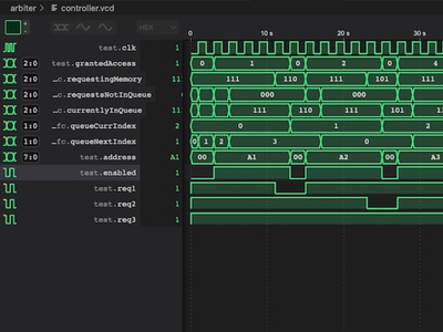
Running make test in a terminal from this folder will create our adc.vcd file where we can see our I2C module working correctly:
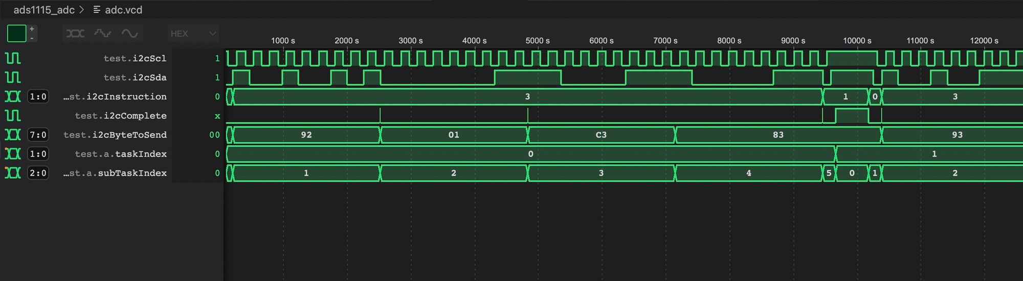
You can see how the task / sub task indices increment sort of like a program counter in a processor through the conversion process and our i2C instruction jumps around between the 4 sub instructions more like how an ALU or cpu handles instructions.
We can also see how the different sub tasks all get combined together to create full i2c transactions over the SDA and SCL lines.
Testing it With The ADS1115
The last thing we are going to do in this article is test it on the tang nano 9k with the ADS1115 connected to see that everything is working.
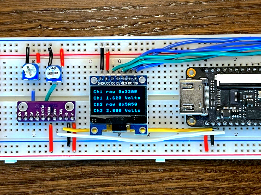
We will create a simple top module that goes back and forth between reading channel 1 or channel 2 from the ADS1115 and then we can display both the raw hex value as well as the value in volts.
To get started let's create a file called top.v with the following:
`default_nettype none

module toHex(
    input clk,
    input [3:0] value,
    output reg [7:0] hexChar = "0"
);
    always @(posedge clk) begin
        hexChar <= (value <= 9) ? 8'd48 + value : 8'd55 + value;
    end
endmodule

module toDec(
    input clk,
    input [11:0] value,
    output reg [7:0] thousands = "0",
    output reg [7:0] hundreds = "0",
    output reg [7:0] tens = "0",
    output reg [7:0] units = "0"
);
    reg [15:0] digits = 0;
    reg [11:0] cachedValue = 0;
    reg [3:0] stepCounter = 0;
    reg [3:0] state = 0;

    localparam START_STATE = 0;
    localparam ADD3_STATE = 1;
    localparam SHIFT_STATE = 2;
    localparam DONE_STATE = 3;

    always @(posedge clk) begin
        case (state)
            START_STATE: begin
                cachedValue <= value;
                stepCounter <= 0;
                digits <= 0;
                state <= ADD3_STATE;
            end
            ADD3_STATE: begin
                digits <= digits +
                    ((digits[7:4] >= 5) ? 16'd48 : 16'd0) +
                    ((digits[3:0] >= 5) ? 16'd3 : 16'd0) +
                    ((digits[11:8] >= 5) ? 16'd768 : 16'd0) +
                    ((digits[15:12] >= 5) ? 16'd12288 : 16'd0);
                state <= SHIFT_STATE;
            end
            SHIFT_STATE: begin
                digits <= {digits[14:0],cachedValue[11] ? 1'b1 : 1'b0};
                cachedValue <= {cachedValue[10:0],1'b0};
                if (stepCounter == 11)
                    state <= DONE_STATE;
                else begin
                    state <= ADD3_STATE;
                    stepCounter <= stepCounter + 1;
                end
            end
            DONE_STATE: begin
                thousands <= 8'd48 + digits[15:12];
                hundreds <= 8'd48 + digits[11:8];
                tens <= 8'd48 + digits[7:4];
                units <= 8'd48 + digits[3:0];
                state <= START_STATE;
            end
        endcase
    end
endmodule
These are the modules we created to convert binary numbers to ASCII hex representation or decimal representation. You can find more info on them in the article where we made them here.
The only difference here is that we added another digit extra so that we can display the voltage as 4 digits.
Next we have our top module:
module top
#(
  parameter STARTUP_WAIT = 32'd10000000
)
(
    input clk,
    output ioSclk,
    output ioSdin,
    output ioCs,
    output ioDc,
    output ioReset,
    inout i2cSda,
    output i2cScl
);

endmodule
The startup wait is for our screen module and besides for that we have the ports for our OLED screen and the 2 wires which we will connect to the ADS1115.
We can setup our screen and text engine modules as follows:
wire [9:0] pixelAddress;
wire [7:0] textPixelData;
wire [5:0] charAddress;
reg [7:0] charOutput = "A";

screen #(STARTUP_WAIT) scr(
    clk,
    ioSclk,
    ioSdin,
    ioCs,
    ioDc,
    ioReset,
    pixelAddress,
    textPixelData
);

textEngine te(
    clk,
    pixelAddress,
    textPixelData,
    charAddress,
    charOutput
);
Our text engine from here allows us set the character we want on screen for each index into charOutput and it will handle drawing the character and interfacing with the OLED screen.
Next we can instantiate our i2c and adc modules, this is pretty much exactly like how we did it in the testbench:
wire [1:0] i2cInstruction;
wire [7:0] i2cByteToSend;
wire [7:0] i2cByteReceived;
wire i2cComplete;
wire i2cEnable;

wire sdaIn;
wire sdaOut;
wire isSending;
assign i2cSda = (isSending & ~sdaOut) ? 1'b0 : 1'bz;
assign sdaIn = i2cSda ? 1'b1 : 1'b0;

i2c c(
    clk,
    sdaIn,
    sdaOut,
    isSending,
    i2cScl,
    i2cInstruction,
    i2cEnable,
    i2cByteToSend,
    i2cByteReceived,
    i2cComplete
);

reg [1:0] adcChannel = 0;
wire [15:0] adcOutputData;
wire adcDataReady;
reg adcEnable = 0;

adc #(7'b1001001) a(
    clk,
    adcChannel,
    adcOutputData,
    adcDataReady,
    adcEnable,
    i2cInstruction,
    i2cEnable,
    i2cByteToSend,
    i2cByteReceived,
    i2cComplete
);
Next we have what will drive the adc module, like mentioned we want to have both the raw value and the value in volts so we can create registers for that:
reg [15:0] adcOutputBufferCh1 = 0;
reg [15:0] adcOutputBufferCh2 = 0;
reg [11:0] voltageCh1 = 0;
reg [11:0] voltageCh2 = 0;

localparam STATE_TRIGGER_CONV = 0;
localparam STATE_WAIT_FOR_START = 1;
localparam STATE_SAVE_VALUE_WHEN_READY = 2;

reg [2:0] drawState = 0;
After the registers which will hold the raw 16-bit value for each channel and registers to store the voltage level we have some states for a state machine:
always @(posedge clk) begin
    case (drawState)
        STATE_TRIGGER_CONV: begin
            adcEnable <= 1;
            drawState <= STATE_WAIT_FOR_START;
        end
        STATE_WAIT_FOR_START: begin
            if (~adcDataReady) begin
                drawState <= STATE_SAVE_VALUE_WHEN_READY;
            end
        end
        STATE_SAVE_VALUE_WHEN_READY: begin
            if (adcDataReady) begin
                adcChannel <= adcChannel[0] ? 2'b00 : 2'b01;
                if (~adcChannel[0]) begin
                    adcOutputBufferCh1 <= adcOutputData;
                    voltageCh1 <= adcOutputData[15] ?
                        12'd0 : adcOutputData[14:3];
                end
                else begin
                    adcOutputBufferCh2 <= adcOutputData;
                    voltageCh2 <= adcOutputData[15] ?
                        12'd0 : adcOutputData[14:3];
                end
                drawState <= STATE_TRIGGER_CONV;
                adcEnable <= 0;
            end
        end
    endcase
end
The first state triggers a conversion by setting the adcEnable flag high, then we wait for the adc to be busy as to make sure we don't read the adcDataReady high value from the previous conversion.
In the last step we wait for the ADC module to finish and return the raw conversion value, and then depending on which channel we were currently doing we store the raw value and the value in volts in their respective registers.
Once we store a value we immediately start a new conversion this time on the other channel.
But let's take another look at the code which sets the voltage:
voltageCh1 <= adcOutputData[15] ? 12'd0 : adcOutputData[14:3];The number we receive is a signed 16-bit number and we are not using negative voltages so we basically have an unsigned 15-bit number. Because of small fluctuations in the conversion even though we are only using the positive side we sometimes may get a negative number close to zero instead of zero. To fix this we can just check if the 16th-bit is high (in which case the signed number is negative) and we will just set the value to zero.
The other interesting thing here is to convert the number from the equation we saw in the ADS1115 datasheet to decimal volts we simply take bit 4 to bit 15. From the datasheet we know the equation to convert values for positive voltages is:
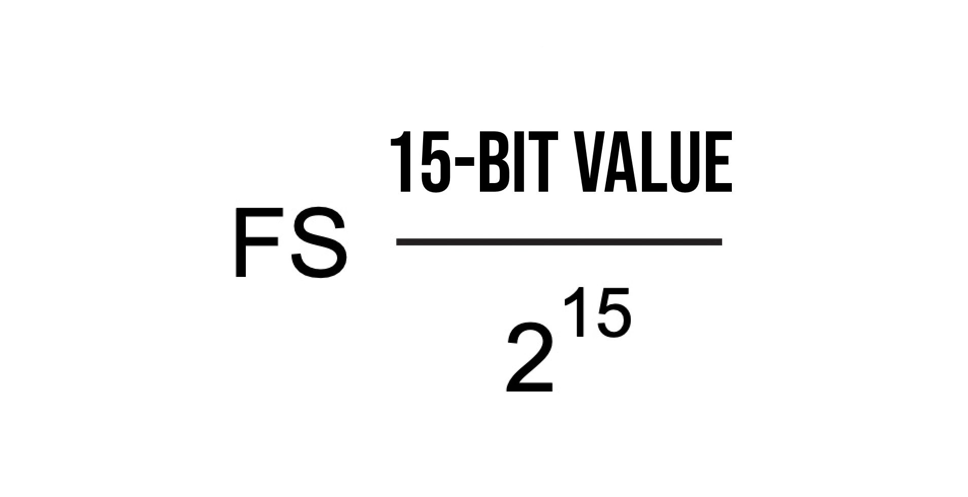
And we set our FS value to 4.096 volts in the config register. The reason this number is so specific and not just 4 volts is because if we multiply the number by 1000 we get a power of two, 212 to be exact. So if we are multiplying by 212 and dividing by 215 then we are left with only a division of 2(15-12) = 23. Dividing by a power of two is simply removing the same amount of lower bits so in our case we simply remove the last 3 bits and take bits 4 to 15 as our voltage and because we multiplied our voltage by 1000 we will have exactly 3 decimal points.
This shouldn't be confused with floating point numbers which are stored completely separately, here we are dealing with fixed point numbers, which is where you are working with integers, but you multiply the number by some factor so you have a fixed number of decimal places.
Again this only works because we multiplied by 1000 to get a power of 2, if we would have only wanted 2 decimal places and only wanted to multiply by 100, then 409 is not a power of 2 and we would need to perform the actual math equation of multiplying the 15-bit value by 409 and then dividing by 215 (or removing the lower 15 bits after the multiplication).
Displaying the Results
Now that we are constantly retrieving conversion values for both channels the last thing we need to do is display the results on screen.
For converting the binary numbers into hex and decimal ASCII representations we will be using our modules toHex and toDec. We can start with the hex characters:
genvar i;
generate
    for (i = 0; i < 4; i = i + 1) begin: hexValCh1
        wire [7:0] hexChar;
        toHex converter(clk, adcOutputBufferCh1[{i,2'b0}+:4], hexChar);
    end
endgenerate
generate
    for (i = 0; i < 4; i = i + 1) begin: hexValCh2
        wire [7:0] hexChar;
        toHex converter(clk, adcOutputBufferCh2[{i,2'b0}+:4], hexChar);
    end
endgenerate
We have a generate block to generate the verilog for 4 hex characters per channel. We have a 16-bit value and each hex character is 4-bits which is why we need 4 characters. The code is simply duplicated once for each channel.
Next a very similar story to convert the voltage into decimal ASCII representation:
wire [7:0] thousandsCh1, hundredsCh1, tensCh1, unitsCh1;
wire [7:0] thousandsCh2, hundredsCh2, tensCh2, unitsCh2;

toDec dec(
    clk,
    voltageCh1,
    thousandsCh1,
    hundredsCh1,
    tensCh1,
    unitsCh1
);

toDec dec2(
    clk,
    voltageCh2,
    thousandsCh2,
    hundredsCh2,
    tensCh2,
    unitsCh2
);
Last but not least we will have an always block which will look at which character is being requested by the text engine based on the screen position being updated and we will place the correct character to display into charOutput.
wire [1:0] rowNumber;
    assign rowNumber = charAddress[5:4];
    always @(posedge clk) begin
        if (rowNumber == 2'd0) begin
            case (charAddress[3:0])
                0: charOutput <= "C";
                1: charOutput <= "h";
                2: charOutput <= "1";
                4: charOutput <= "r";
                5: charOutput <= "a";
                6: charOutput <= "w";
                8: charOutput <= "0";
                9: charOutput <= "x";
                10: charOutput <= hexValCh1[3].hexChar;
                11: charOutput <= hexValCh1[2].hexChar;
                12: charOutput <= hexValCh1[1].hexChar;
                13: charOutput <= hexValCh1[0].hexChar;
                default: charOutput <= " ";
            endcase
        end
        else if (rowNumber == 2'd1) begin
            case (charAddress[3:0])
                0: charOutput <= "C";
                1: charOutput <= "h";
                2: charOutput <= "1";
                4: charOutput <= thousandsCh1;
                5: charOutput <= ".";
                6: charOutput <= hundredsCh1;
                7: charOutput <= tensCh1;
                8: charOutput <= unitsCh1;
                10: charOutput <= "V";
                11: charOutput <= "o";
                12: charOutput <= "l";
                13: charOutput <= "t";
                14: charOutput <= "s";
                default: charOutput <= " ";
            endcase
        end
        else if (rowNumber == 2'd2) begin
            case (charAddress[3:0])
                0: charOutput <= "C";
                1: charOutput <= "h";
                2: charOutput <= "2";
                4: charOutput <= "r";
                5: charOutput <= "a";
                6: charOutput <= "w";
                8: charOutput <= "0";
                9: charOutput <= "x";
                10: charOutput <= hexValCh2[3].hexChar;
                11: charOutput <= hexValCh2[2].hexChar;
                12: charOutput <= hexValCh2[1].hexChar;
                13: charOutput <= hexValCh2[0].hexChar;
                default: charOutput <= " ";
            endcase
        end
        else if (rowNumber == 2'd3) begin
            case (charAddress[3:0])
                0: charOutput <= "C";
                1: charOutput <= "h";
                2: charOutput <= "2";
                4: charOutput <= thousandsCh2;
                5: charOutput <= ".";
                6: charOutput <= hundredsCh2;
                7: charOutput <= tensCh2;
                8: charOutput <= unitsCh2;
                10: charOutput <= "V";
                11: charOutput <= "o";
                12: charOutput <= "l";
                13: charOutput <= "t";
                14: charOutput <= "s";
                default: charOutput <= " ";
            endcase
        end
    end
We handle each row separately, for each row we have a case statement where we choose the correct character to display based on the current column.
Hooking up the ADS1115
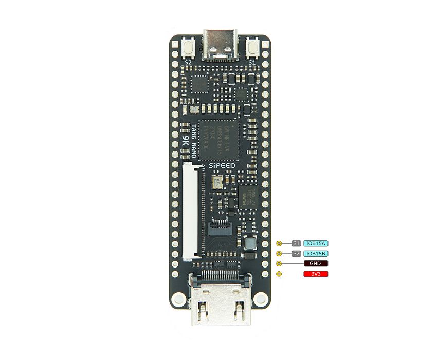
Taking a look at the pinout of the ADS1115 again:

We need to connect the top two pins to 3.3v and ground and the next two pins need to be connected to the tang nano. We can get these 4 pins from here on the tang nano:
So let us create our constraints file, tangnano9k.cst
IO_LOC "clk" 52;
IO_PORT "clk" IO_TYPE=LVCMOS33 PULL_MODE=UP;

IO_LOC "ioCs" 36;
IO_PORT "ioCs" IO_TYPE=LVCMOS33 PULL_MODE=DOWN DRIVE=8;
IO_LOC "ioDc" 39;
IO_PORT "ioDc" IO_TYPE=LVCMOS33 PULL_MODE=DOWN DRIVE=8;
IO_LOC "ioReset" 25;
IO_PORT "ioReset" IO_TYPE=LVCMOS33 PULL_MODE=DOWN DRIVE=8;
IO_LOC "ioSdin" 26;
IO_PORT "ioSdin" IO_TYPE=LVCMOS33 PULL_MODE=DOWN DRIVE=8;
IO_LOC "ioSclk" 27;
IO_PORT "ioSclk" IO_TYPE=LVCMOS33 PULL_MODE=DOWN DRIVE=8;

IO_LOC "i2cSda" 31;
IO_PORT "ioSclk" IO_TYPE=LVCMOS33;
IO_LOC "i2cScl" 32;
IO_PORT "ioSclk" IO_TYPE=LVCMOS33;
The first group is the clock, then we have the 5 lines for controlling the OLED screen and finally our 2 I2C pins, pin 31 for SDA and pin 32 for SCL.
Next we need to connect the ADDR pin on the ADS1115 board to 3.3v as-well in-order to set the I2C address to 7'b1001001.
Other then that you need to connect analog values between 0-3.3v to the analog channels you want to use (in our case the first two channels). I will be using a potentiometer for this. So you connect one side of the potentiometer to 3.3v the other side to ground and the sweeper pin will move between the two voltages as you turn the potentiometer.
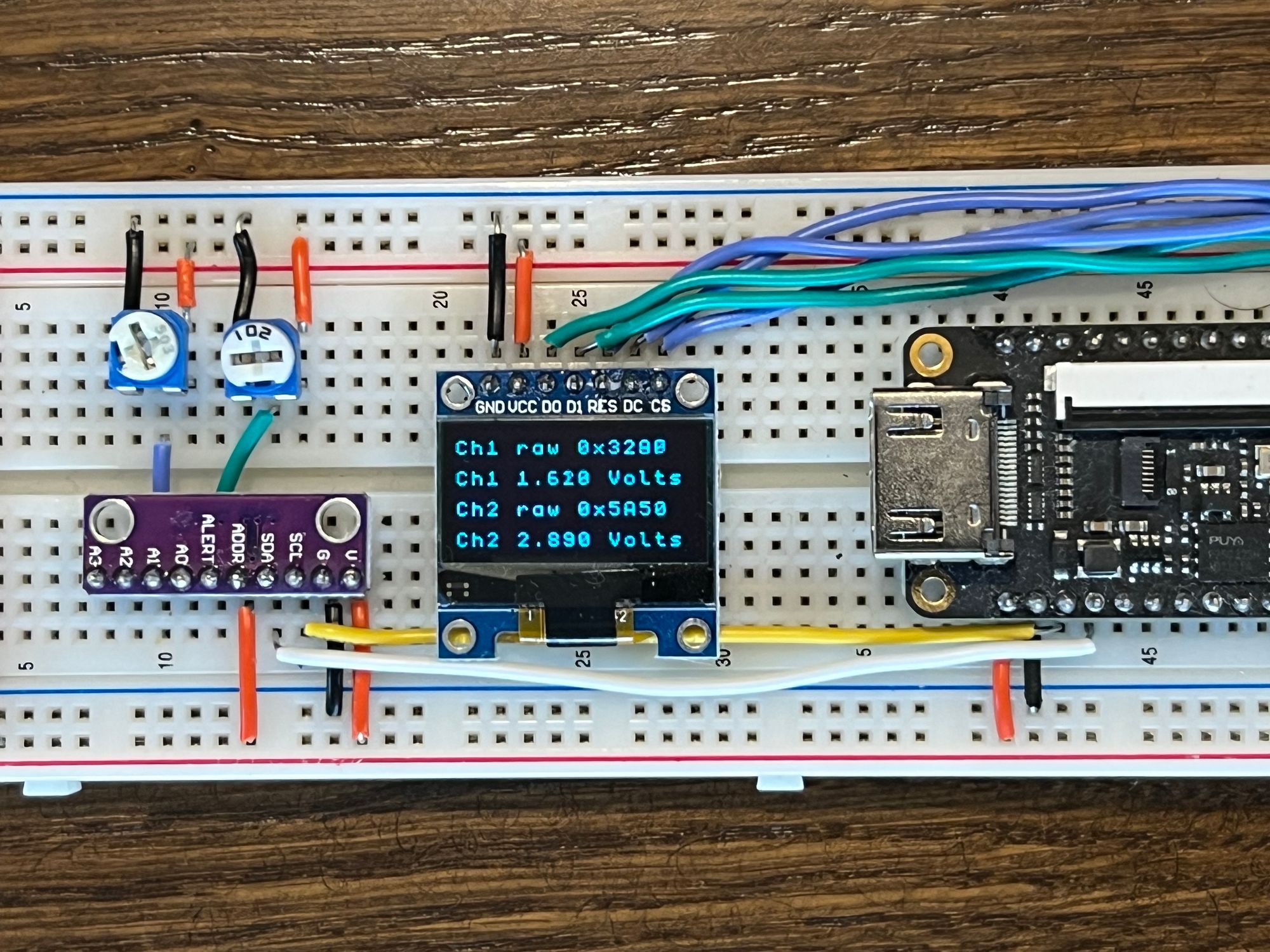
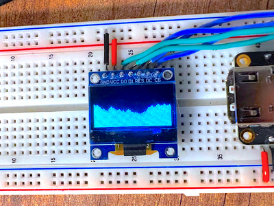
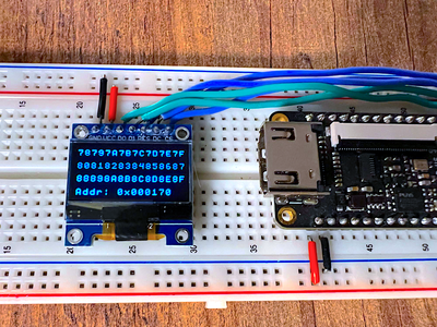
With everything wired up you can program the tang nano by running make load which will both synthesize and program the tang nano 9k. You should see something like the following:
Conclusion
In this article we explored the ADS1115 ADC, the I2C protocol and hopefully a more general approach that can be used to implement a new core. As a rule of thumb if something is complicated to explain or implement then you are usually dealing with a compound task and breaking it up into sub tasks / building blocks can make it a lot simpler and easier.
This article is longer then are regular format, so if you made it to the end then you are definitely a real one, I want to thank you for reading and I hope you enjoyed it.
Like always if you have any questions or comments feel free to leave them in the comments below or on twitter @LushayLabs
If you would like to purchase any of the hardware used in this article like the Tang Nano, OLED or ADS1115 board you can visit our store here.
The code along with the code from all our articles in the TangNano series can be found on github here
