
This is a new section on our site for more general projects, as opposed to the main tang nano 9K series where we try to only use the OS toolchain and components available in our store to make sure they are accessible to everyone, in this series we want to remove all restrictions and showcase interesting and cool projects from us and the community.
We are very excited to release our first community project - Project EDID - brought to us by Jeroen Wolf and Martijn Backus, experts in the A/V industry, so special thanks to them for providing both the idea and all the technical info required to create this project.
The Concept
When setting up systems with multiple displays (this can be monitors, projectors, etc.) you need to know some basic information about each display to make sure you set everything up in a way that is compatible for each display. For example if a screen doesn't support 4K resolution and you try to supply it such a signal it won't know how to handle it.
In more complex setups you may have many monitors with splitters duplicating the image on differently sized monitors. Even in simpler cases think of a large classroom setup where there may have multiple projectors for the students and a second monitor for the teacher. Here you would use a device which could duplicate the signal to all these sources, but the driving computer would need to be set to a resolution compatible with all devices.
In these kinds of situations it would be cool to have a small & portable device (as opposed to carrying around a laptop) that can detect and display this info for each screen so that you can quickly & easily make these decisions while at a job site.
How does it work?
The first question is how does your computer communicate and know what resolution to use for each display. If you have ever connected a monitor (or second monitor for laptops) you don't need to manually adjust the resolution for it to work, your computer will automatically know what resolutions are supported and what the preferred resolution of the display is.
The way this works is that each screen stores this info (and more) in a byte structure format in a standard called EDID or Extended Display Identification Data. This data is read by the host device over I2C when connected and then is decoded to retrieve all this info.
There are multiple versions of EDID but all the new revisions seem to be compatible at least in regards to the data we will be extracting. The format we will be basing our design on is EDID 2.0 or E-EDID 1.4 which uses a 256 byte format.

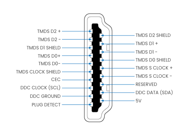
Electronically like I said the data is transferred via I2C, the host device sends a read command to read from a specific address and the screen replies with the EDID bytes. This doesn't happen over the standard pins used to transfer video, it happens over dedicated pins that form what is called the DDC (Data display channel) but essentially for us it is a standard 5V I2C channel with SDA / SCL.
In our example we'll be keeping it simple and we won't be decoding everything the EDID has to offer. Instead we will be reading the screen's name and the screen's preferred resolution along with the refresh rate. If you are interested in learning more about what is stored in the EDID I would recommend checking out the page on wikipedia page or this detailed spec which details what is stored in the other bytes.
Decoding the EDID
Before getting into the implementation, let's first take a look at where the data we need is located in the EDID and the format it is in.
Taking a look at the structure of the first 127 bytes:
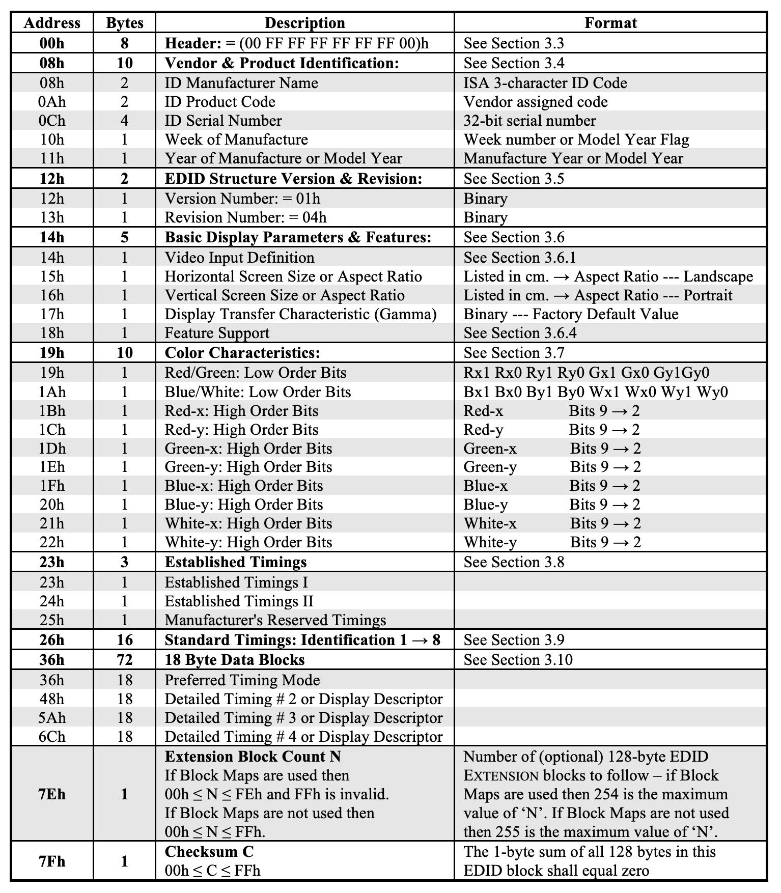
You can see that the block starts off with a fixed 8 byte header to identify standard and then another 46 bytes defining:
- vendor / product identifiers
- EDID version
- Basic Display specs
- Color info
- Timings
This is followed by four descriptors each 18 bytes long, each descriptor can be used to hold a specific kind of information. The first descriptor is used to hold the prefered resolution of the screen and each descriptor starts off with a type that can be used to identify the kind of information stored in the other 3.
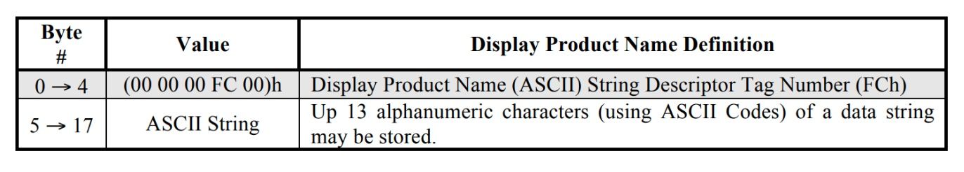
The name of the screen is stored in one of these 3 descriptors and is denoted by a 5 byte prefix of 0x000000FC00 and then the remaining 13 bytes are used to store up to 13 ASCII characters.
For the prefered resolution, like we saw this is stored in the first descriptor block and uses a slightly more complicated structure:
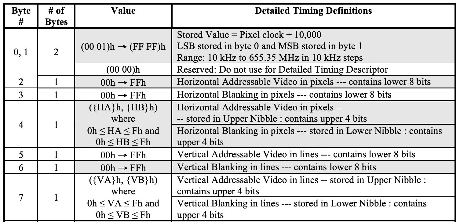
The timing descriptor has 18 bytes but we only need the first 8. The first thing we need is the pixel clock rate, this is a 16-bit number representing the pixel clock rate in 10Khz steps. So for example a value of 500 would be 500 * 10kHz which is 5000kHz or 5Mhz, meaning 5,000,000 "pixels" would be sent a second.
Now looking at the value column for the other fields may seem complicated at first, but essentially what is going on here is that the format stores 2 12-bit numbers as two 8-bit numbers and then combines the other 4 bits from each of these numbers into a 3rd byte.
So for example Byte #2 stores the bottom 8-bits of the horizontal video pixels count and byte #3 stores the bottom 8-bits of the horizontal blanking pixels count, and then byte #4 stores both their 4-upper bits. So the top 4-bits of byte #4 are the top 4-bits for the horizontal video pixel count and the bottom 4-bits of byte #4 are the top 4-bits for the horizontal blanking pixels count.
So for example if these 3 bytes were:
- Byte #2:
0x1F - Byte #3:
0x2E - Byte #4:
0x3D
Then you would split byte #4 into two 4-bit numbers, so it would become 0x3 and 0xD and then add them at the top of the other two bytes. So the horizontal video pixel count would be 0x31F and the horizontal blanking pixel count would be 0xD2E.
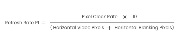
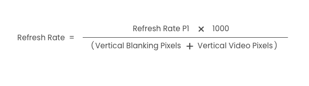
So for the preferred resolution we simply need the horizontal video pixel count and vertical video pixel count, but to calculate the refresh rate of the screen we will need to perform a little math. The refresh rate of the screen is the pixel clock rate from before divided by the number of pixels, which includes both video pixels as well as blanking pixels. So the equation looks something like this:

As a side note, the blanking pixels are a sort of analogy where instead of thinking of HDMI as sending multiple types of data interlaced taking turns between them, you can think of all the data as 1 "larger" image. As bytes are bytes it doesn't really make a difference how you choose to think about them, so instead of splitting it up into video data, audio data and control data you can think of it as 1 larger video picture and just refer to all data as pixels.
So the horizontal blanking pixels are a number of pixel clock pulses that can be used to transmit data other then video pixels around each line, and the vertical blanking pixels are an extra number of full rows where other data can be transmitted.
The horizontal and vertical blanking are really split up into a part before and a part after the video pixels (called the front and back porch respectively), but for our purposes the above image is enough as in our case it is just a matter of reference.
Getting back to our equation:

This poses an interesting resource problem when working with FPGAs, We are adding two 12-bit numbers (the video and blanking pixels) for each direction giving us up to a possible 13-bit number and then we need to multiply these two 13-bit numbers together giving us a possible 26-bit number. The pixel clock itself is stored as a 16-bit number and the value needs to be multiplied by 10,000 to get the actual rate in hertz and screen refresh rates are in hertz like 30 times per second so we can't leave it in 10Khz units or it would always be rounded to 0.
Trying to run this even in a simple example like the following would not work for multiple reasons:
module top(
    input clk,
    input [11:0] horizontalPixels,
    input [11:0] horizontalBlanking,
    input [11:0] verticalPixels,
    input [11:0] verticalBlanking,
    input [15:0] pixelRate,
    output [15:0] refreshRate
);

reg [15:0] temp = 16'd0;
always @(posedge clk) begin
    temp <= (10000 * pixelRate) / (
        (horizontalPixels + horizontalBlanking) * (verticalPixels + verticalBlanking)
    );
end
assign refreshRate = temp;

endmodule
Running this like this puts a strain on resources both in terms of timing, since we require the entire operation to complete within a single clock pulse making it not so flexible in terms of placement and it also takes up about 40-50% of the system resources:
I think this is a good illustration of the difference between programming software and programming hardware. In software you would write an operation like this and it would be split up into sub-operations each one taking x number of clock cycles, you don't really need to deal with it. In software the CPU has an ALU which can for example take two 32-bit numbers and choose to either multiply, divide add or subtract them. So this equation would be handled on the same physical ALU one at a time.
So again, both in terms of time and in terms of physical resources used everything is taken care of for you. In hardware programming, writing verilog like this means you are dedicating hardware resources for all parts of the equation to work in parallel and for the entire process to complete in a single clock pulse limiting the rest of your design.
So besides for extracting the EDID information from the screen we will need to think of a way to calculate this more efficiently.
Some Setup
For this project we will be using some modules from previous articles, you can download the starter for this project with these files here
The modules we will be importing are:
- screen.v - Contains the OLED driver - full article here
- text.v - Allows us to draw text to the screen - full article here
- todec.v - Converts binary numbers to separate ascii digits - full article here
- i2c.v - The I2C Driver - full article here
With those files in place we can start creating the edid module itself.
The Implementation
Reading the Edid data is actually quite simple. We start an I2C transaction and send a write command to address 0x50, this is the I2C address to access the EDID "ROM", next we can send another byte over I2C to tell it where in the EDID to start reading from.
Once we set the byte index to read from, we can restart the I2C transaction this time with a read command to address 0x50, after which we can continue to read the entire EDID one byte at a time. In pseudo code it would look something like the following:
i2c_start_tx()
i2c_write_command(0x50)		// address for EDID
i2c_write_byte(0x00) 		//start reading from byte 0
i2c_start_tx()
i2c_read_command(0x50)
for (let i = 0; i < 256; i += 1) {
	i2c_read_byte()
}
i2c_stop_tx()
Where if you remember from the previous I2C article both i2c_write_command and i2c_read_command are essentially just i2c_write_byte with a 7-bit address and the last bit is used to differentiate between reading and writing.
For simplicity I would probably read the entire EDID into RAM and then work on it from there, but RAM support for such a large amount of bytes is kind of dodgy using the open source toolchain, so for this example we will be processing the bytes as we read them.
It is also worth noting that the default byte index is zero, so we could have probably skipped the write operation altogether and just starting reading, but it doesn't hurt to add it just to make sure that if for example we reset the read operation in the middle that we reset the byte index to zero.
With the theory done we can create a new file called edid.v where we can start creating our module:
module edid (
    input clk,
    input enable,
    output reg dataReady = 1,

    output reg [1:0] instructionI2C = 0,
    output reg enableI2C = 0,
    output reg [7:0] byteToSendI2C = 0,
    input [7:0] byteReceivedI2C,
    input completeI2C,

    input [3:0] charIndex,
    input [1:0] rowIndex,
    output reg [7:0] edidDataOut = 0,
);

endmodule
We can split the ports into 3 groups, first off we have the clock signal input, an enable input to start the EDID processing and a flag bit output where this module can signal that the EDID processing is complete.
Next we have the 5 ports needed to interface with our I2C module. We have the instruction register where we can set which I2C operation we would like to perform and we have the enable bit to start a new operation, besides that we have a register which stores a byte for each direction (for sending a byte and for receiving a byte over I2C) and finally the complete signal from the I2C to know that the operation has completed.
The last group of ports is to output the data to the screen. Instead of passing all the values that we would like to display, like the name, resolution and refresh rate, it is less resource intensive to just pass the current character that we would like to display when needed. So we have the row and column index on the screen that is currently being drawn and then we can output the desired ASCII character via edidDataOut.
Next we can add localparams for the I2C instructions just for convenience:
localparam INST_START_TX = 0;
localparam INST_STOP_TX = 1;
localparam INST_READ_BYTE = 2;
localparam INST_WRITE_BYTE = 3;
We need to put one of these values into the instructionI2C register and set the enable bit to start an I2C operation.
Next we can add the states we will be using in our state machine:
localparam STATE_IDLE = 0;
localparam STATE_START_I2C = 1;
localparam STATE_SEND_ADDRESS = 2;
localparam STATE_SEND_EDID_BYTE_INDEX = 3;
localparam STATE_RESTART_I2C_FOR_READ = 4;
localparam STATE_SEND_READ_COMMAND = 5;
localparam STATE_HANDLE_BYTES = 6;
localparam STATE_READ_BYTE = 7;
localparam STATE_NEXT_READ_NAME = 8;
localparam STATE_STOP_I2C = 9;
localparam STATE_REFRESH_RATE = 10;
localparam STATE_REFRESH_RATE2 = 11;
localparam STATE_REFRESH_RATE3 = 12;
localparam STATE_REFRESH_RATE4 = 13;
localparam STATE_DONE = 14;
localparam STATE_WAIT_FOR_I2C = 15;
It may look like a lot of states but each state is relatively simple. We start off in the idle state, and when we receive the signal to start processing the EDID then we move to the START_I2C state in order to start the I2C communication.
Then like in the pseudo code we have states for sending the I2C write command to address 0x50 called STATE_SEND_ADDRESS followed by the state which will send the byte index inside the EDID where we would like to start reading from.
With the two write operations done we will use the next state to restart the I2C communication and the send a read command using the STATE_SEND_READ_COMMAND which again is just sending a byte over I2C with the address 0x50 and the last bit tells the I2C device that we would like to read.
From here all the setup is done and we start reading and handling the EDID bytes using the HANDLE_BYTES state. Theoretically this could have been the end, but as we saw above there are three separate locations where the screen name could be stored (in descriptor 2,3 or 4) so instead of adding special logic to handle this in the HANDLE_BYTES state I decided to just wait until we identify the prefix telling us that we found the descriptor containing the screen name and then we will branch off into a separate state which will know to read the 13 characters storing the name.
This works also because all the other info we need like the number of pixels and timings occur before the name descriptor in the EDID so once we get to the name we can simply branch off, handle the name and finish the I2C connection.
That is what the next 3 states are doing, we are reading 1 of these 13 name bytes and storing them in a register after which we are stopping the I2C communication as we have all the data we need from the screen.
The next 4 states all labeled REFRESH_RATE are to handle the large equation we spoke about. By splitting it up into multiple separate stages and clock cycles it allows us to simplify the timing and resource requirements.
After this we have the DONE state where we will signal that we have completed the EDID processing and finally the last state is just a helper state where we can wait for the current I2C sub-operation to complete before advancing our state machine.
Next in terms of registers we will need something to store the state we are in as well as the state we want to return to after I2C operations:
reg [3:0] state = STATE_IDLE;
reg [3:0] returnState = 0;
reg processStarted = 0;
processStarted will allow us to keep track of the current sub I2C operation.
Next we need some registers to store the pieces of information we will be extracting from the EDID:
reg [103:0] screenName = 0;
reg [11:0] horizontalPixels = 0;
reg [11:0] verticalPixels = 0;
reg [15:0] pixelClock = 0;
reg [11:0] horizontalBlank = 0;
reg [11:0] verticalBlank = 0;
reg [11:0] refreshRate = 0;
And finally we need some helper registers:
reg [3:0] nameCounter = 0;
reg [7:0] counter = 0;
reg [19:0] refreshCalcTop = 0, refreshCalcBottom = 0;
reg [2:0] foundNamePrefix = 0;
nameCounter will allow us to keep track of how many of the 13 name characters we have read, counter we will use as a general purpose register. refreshCalcTop and refreshCalcBottom will store the numerator and denominator of the refresh rate calculation and finally foundNamePrefix will allow us to count how many of the 5 byte prefix which tells us that the current descriptor is the screen name are matching.
If any of that was unclear I think seeing the implementation of the state machine might help clear it up.
The State Machine
Like usual for our state machine we will begin with an always block and a case statement:
always @(posedge clk) begin
    case (state)
    	// states here
    endcase
end
Our first idle state just waits for the enable signal to come in:
STATE_IDLE: begin
    if (enable) begin
        state <= STATE_START_I2C;
        dataReady <= 0;
        nameCounter <= 0;
        counter <= 0;
        refreshRate <= 0;
        foundNamePrefix <= 0;
    end
end
As soon as enable goes high we reset our state registers and move to the START_I2C state. In the next state we want to interface with our I2C module:
STATE_START_I2C: begin
    instructionI2C <= INST_START_TX;
    enableI2C <= 1;
    state <= STATE_WAIT_FOR_I2C;
    returnState <= STATE_SEND_ADDRESS;
end
Like mentioned we simply need to set the instruction and enable bit to start our I2C module. We then go to our waiting state which we will get to a little later, but once the operation is complete we return to the next state which is the SEND_ADDRESS state.
STATE_SEND_ADDRESS: begin
    instructionI2C <= INST_WRITE_BYTE;
    byteToSendI2C <= {7'h50, 1'b0};
    enableI2C <= 1;
    state <= STATE_WAIT_FOR_I2C;
    returnState <= STATE_SEND_EDID_BYTE_INDEX;
end
Sending the I2C write command is a matter of writing to the I2C bus a byte where the first 7 bits contain the address of the device we want to communicate with (our 0x50 address) and the final bit tells it if we would like to read or write, zero being write and a one there would have meant read.
STATE_SEND_EDID_BYTE_INDEX: begin
    instructionI2C <= INST_WRITE_BYTE;
    byteToSendI2C <= 0;
    enableI2C <= 1;
    state <= STATE_WAIT_FOR_I2C;
    returnState <= STATE_RESTART_I2C_FOR_READ;
end
Next we send the byte index where we want to start reading from in the EDID. We are sending zero so that it starts at the beginning.
With the write operations out of the way we can restart the communication channel to move to reading:
STATE_RESTART_I2C_FOR_READ: begin
    instructionI2C <= INST_START_TX;
    enableI2C <= 1;
    state <= STATE_WAIT_FOR_I2C;
    returnState <= STATE_SEND_READ_COMMAND;
end
This just sends another start tx event on the I2C line like in the START_I2C state and next we need to send a read command:
STATE_SEND_READ_COMMAND: begin
    instructionI2C <= INST_WRITE_BYTE;
    byteToSendI2C <= {7'h50, 1'b1};
    enableI2C <= 1;
    state <= STATE_WAIT_FOR_I2C;
    returnState <= STATE_HANDLE_BYTES;
end
Here you can see that after the 7-bit address we are sending a 1 in the last bit to signify reading.
The next state is where most of the EDID parsing happens. We start off relatively the same but we add an internal case statement to process each byte as we read it.
STATE_HANDLE_BYTES: begin
    instructionI2C <= INST_READ_BYTE;
    enableI2C <= 1;
    state <= STATE_WAIT_FOR_I2C;
    returnState <= STATE_HANDLE_BYTES;
    counter <= counter + 1;

    case (counter)
        // handle bytes here
        default: begin end
    endcase
end
Basically in each iteration we will read a byte over I2C using our I2C module's READ_BYTE instruction returning to here. We then use the counter to understand which byte is currently in the byteReceivedI2C register and handle it in the internal case statement.
Now inside the internal case statement (not to be confused with our outer state machine case statement) we need to add the byte handling:
1, 8: begin
    if (byteReceivedI2C != 8'h00) begin
        state <= STATE_IDLE;
        enableI2C <= 0;
    end
end
The edid is meant to start an 8 byte prefix where the 1st and last bytes are zeros and all the bytes in between are 0xFF. I decided just to check the first and last, since I2C has a pull up resistor, so the default value is 0xFF making the byte checks for the 0x00 bytes more meaningful to me. You could of course have added checks for both, but to keep it simple I just checked these 2 bytes from the prefix.
If we are on byte 1 or byte 8 we make sure that the byte received over I2C equals 0x00 as per the EDID spec, if not we go back to IDLE restarting the EDID processing since something has gone wrong (or the screen is not connected).
Now for the actual data if we look back at our diagram for the timing descriptor:

The first thing we can extract from timing descriptor 1 is the pixel clock which is a 16-bit number where byte 0 is the least significant byte and byte 1 is the most significant byte. In our internal case statement this would look like this:
55: pixelClock[7:0] <= byteReceivedI2C;
56: pixelClock[15:8] <= byteReceivedI2C;
The first timing descriptor starts at byte index 54 and we started our index at 1 instead of zero (since the first loop inside of HANDLE_BYTES is before we read the first byte) so for us byte index 54 is byte number 55.
Next we have the horizontal pixel size:
57: horizontalPixels[7:0] <= byteReceivedI2C;
58: horizontalBlank[7:0] <= byteReceivedI2C;
59: begin
    horizontalPixels[11:8] <= byteReceivedI2C[7:4];
    horizontalBlank[11:8] <= byteReceivedI2C[3:0];
end
Like we spoke about, these are 12-bit numbers where the lower byte is stored for each variable separately, but then the two variable's upper 4-bits are combined together in the next byte.
We have the same exact thing for the vertical pixels:
60: verticalPixels[7:0] <= byteReceivedI2C;
61: verticalBlank[7:0] <= byteReceivedI2C;
62: begin
    verticalPixels[11:8] <= byteReceivedI2C[7:4];
    verticalBlank[11:8] <= byteReceivedI2C[3:0];
end
And with that we have read all the info we need except for the screen's name. For the screen name we need to first find which descriptor starts off with 0x000000FC00. The relevant descriptors start at bytes 73, 91 or 109 and basically we are looking for the first 3 bytes to all be 0x00 so we can do that with the following check:
73, 74, 75,
91, 92, 93,
109, 110, 111: foundNamePrefix <= byteReceivedI2C === 8'h00 ?
                   foundNamePrefix + 1 : 0;
These are all the byte numbers for the first three bytes of each descriptor, for each of these bytes if they are 0x00 then we increment the foundNamePrefix counter. The next byte for each of these descriptors is meant to be 0xFC so we can do something similar for them:
76, 94, 112: foundNamePrefix <= byteReceivedI2C === 8'hFC ?
                 foundNamePrefix + 1 : 0;
Just changing what the byte is meant to equal. And for the last byte of the prefix we just check to make sure that it equals 0x00 and also that foundNamePrefix equals 4 meaning the previous 4 bytes of the prefix were also correct:
77, 95, 113: begin
    if (byteReceivedI2C == 8'h00 && foundNamePrefix == 3'd4)
        returnState <= STATE_NEXT_READ_NAME;
    else
        foundNamePrefix <= 0;
end
If we found the correct descriptor then we change the returnState for the next byte read to be the READ_NAME state otherwise we continue in the HANDLE_BYTES state waiting to check the next descriptor.
With that we have finished the internal case statement and can return to the outer case statement where we are implementing our state machine. The next state we can implement is this state where we will be storing the name:
STATE_NEXT_READ_NAME: begin
    screenName[{nameCounter, 3'b0}+:8] <= byteReceivedI2C;
    nameCounter <= nameCounter + 1;
    state <= (nameCounter === 12) ? STATE_STOP_I2C : STATE_READ_BYTE;
end
We use the nameCounter to keep track of where we are in the screen's name and after reading all 13 characters we move to the STOP_I2C state to end the communication. But first let's take a look at the READ_BYTE state which is just another state to trigger an I2C read byte operation like HANDLE_BYTES would do:
STATE_READ_BYTE: begin
    instructionI2C <= INST_READ_BYTE;
    enableI2C <= 1;
    state <= STATE_WAIT_FOR_I2C;
    returnState <= STATE_NEXT_READ_NAME;
end
Nothing new here, just triggering the read byte and returning to the READ_NAME state to store the next character. Now if we did read all 13 bytes of the name then we stop the I2C again with another instruction to our I2C module:
STATE_STOP_I2C: begin
    instructionI2C <= INST_STOP_TX;
    enableI2C <= 1;
    state <= STATE_WAIT_FOR_I2C;
    returnState <= STATE_REFRESH_RATE;
end
We are done with the screen so we stop the transmission, we have all the data we need we just need to do a little processing first to calculate the refresh rate.
Performing the Calculation
We have all the variables for our calculation:

But again this is a lot to handle and would result in large register sizes, we also didn't multiply pixelClockRate by 10,000 to receive the value in Hertz like the final result will be in, and again we need to do this as we don't have fractions and all values would be rounded to zero if not.
To solve this we are going to split up the equation into two parts. The first part being:
And then we can take the results of this and perform the rest of the operation:
We can also split each of these into two steps, where we first calculate the numerator and denominator of each stage and then perform the division. The final thing we are going to do, is we are going to perform the division through subtraction.
So for example if you wanted to know what 30 divided 5 is you can keep subtracting 5 from 30 and count the number of times, in this case you would get to zero (or a number under 5) after 6 subtractions meaning the answer to the division is 6.
So to begin with let's prepare the numerator and denominator for the first calculation:
STATE_REFRESH_RATE: begin
    refreshCalcTop <= pixelClock * 10;
    refreshCalcBottom <= {8'b0, horizontalPixels + horizontalBlank};
    state <= STATE_REFRESH_RATE2;
end
Like in the image above, we multiply our pixel clock by 10 and we add the video pixels and blanking pixels together for the denominator.
In the next state we will be performing the division via subtraction:
STATE_REFRESH_RATE2: begin
     if (refreshCalcTop >= refreshCalcBottom) begin
          refreshCalcTop <= refreshCalcTop - refreshCalcBottom;
          refreshRate <= refreshRate + 1;
     end else begin
          state <= STATE_REFRESH_RATE3;
          refreshCalcBottom <= {8'b0, verticalPixels + verticalBlank};
     end
end
While the numerator is larger than or equal to the denominator we can perform another subtraction, each time incrementing the refreshRate which will store the results of our first calculation.
If we can no longer subtract then we move on to the next state already preparing it's denominator.
STATE_REFRESH_RATE3: begin
    refreshCalcTop <= {8'b0, refreshRate} * 20'd1000;
    refreshRate <= 0;
    state <= STATE_REFRESH_RATE4;
end
In this next state we set the numerator to be the refresh rate multiplied by 1000 completing the conversion of our pixel clock into hertz and we already have the denominator ready so we move onto the final step in our calculation, performing another division.
STATE_REFRESH_RATE4: begin
    if (refreshCalcTop >= refreshCalcBottom) begin
        refreshCalcTop <= refreshCalcTop - refreshCalcBottom;
        refreshRate <= refreshRate + 1;
    end else begin
        if (refreshCalcTop > 0)
            refreshRate <= refreshRate + 1;
        state <= STATE_DONE;
    end
end
Very similar to the first division, while we can still subtract we subtract and once done we have the final refresh rate inside the refreshRate variable. We also check to see if there was any remainder left in the numerator and if so we round up by incrementing the refreshRate register.
Another benefit to calculating it like this is we never needed to store / work with the 26-bit register we talked about which would be required to hold the complete pixel count (original denominator). By dividing by each part separately we kept the overall numbers we were working with small.
Last Two States
With the last piece of info we needed calculated we can node write the DONE state:
STATE_DONE: begin
    dataReady <= 1;
    if (~enable)
        state <= STATE_IDLE;
end
We signal to the top module that we are done processing the edid and we wait for the enable flag to go low to go back to idle. This is so that we don't trigger another EDID processing on the same old enable signal.
The final state is the state which waits for the sub I2C operations to complete. It uses the same design as we just implemented with the DONE state except we are the controlling side:
STATE_WAIT_FOR_I2C: begin
     if (~processStarted && ~completeI2C)
          processStarted <= 1;
     else if (completeI2C && processStarted) begin
          state <= returnState;
          processStarted <= 0;
          enableI2C <= 0;
     end
end
If we have not yet started the action, we wait for the completeI2C flag to go low signifying that the I2C module received the instruction and is now in progress.
Once this happens we shift are focus on waiting for the completeI2C flag to go back high signifying that the conversion is complete. Where we then release the enableI2C flag to let the I2C module go back to it's idle state.
Our state machine is now done and the last thing we need to do here is export the data for the screen module.
Displaying the Data
Displaying the name to the screen is pretty simple, we already have the 13 characters in ascii format, so based on the requested character we can return the character to be displayed. For the other information on screen we need a two step process, we need to convert our binary numbers into ASCII decimal digits, and then based on which character is being requested we need to return one of those characters.
For the conversion we can use our toDec module:
wire [7:0] verticalThousand, verticalHundred, verticalTen, verticalUnit;
wire [7:0] horizontalThousand, horizontalHundred, horizontalTen, horizontalUnit;
wire [7:0] refreshThousands, refreshHundreds, refreshTen, refreshUnit;


toDec vertConv(
    clk,
    horizontalPixels,
    horizontalThousand,
    horizontalHundred,
    horizontalTen,
    horizontalUnit
);
toDec horizConv(
    clk,
    verticalPixels,
    verticalThousand,
    verticalHundred,
    verticalTen,
    verticalUnit
);
toDec refreshConv(
    clk,
    refreshRate,
    refreshThousands,
    refreshHundreds,
    refreshTen,
    refreshUnit
);
We need to create wires to hold each of the ascii characters, 1 character per digit column. Our converter converts numbers with 4 digit columns so we have 4 ASCII bytes per conversion.
Besides for the wires we just add 3 instances of our converter one for the horizontal pixel count 1 for the vertical pixel count and one for the refresh rate.
always @(posedge clk) begin
if (~enable) begin
if (rowIndex == 1)
edidDataOut <= screenName[{charIndex, 3'b0}+:8];
else if (rowIndex == 3) begin
case (charIndex)
0: edidDataOut <= horizontalThousand;
1: edidDataOut <= horizontalHundred;
2: edidDataOut <= horizontalTen;
3: edidDataOut <= horizontalUnit;
5: edidDataOut <= verticalThousand;
6: edidDataOut <= verticalHundred;
7: edidDataOut <= verticalTen;
8: edidDataOut <= verticalUnit;
12: edidDataOut <= refreshTen;
13: edidDataOut <= refreshUnit;
default: edidDataOut <= "";
endcase
end
end
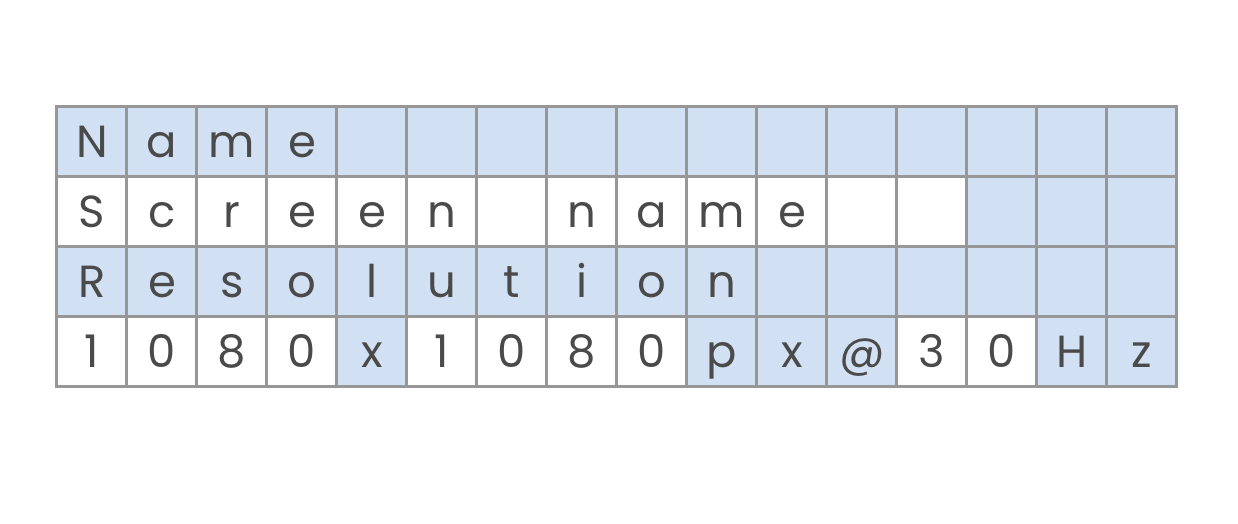
endThis block simply waits for the conversion process to be done by checking that the enable signal is off. If so for line index 1 we return the screen name. And for line index 3 we return the pixel information and refresh rate. If you are wondering why these indexes, the reason is I am aiming for something that looks like the following:

Where all the highlighted cells are static characters and will be filled in by the top module and here we only need to provide the dynamic data like the name and numbers used.
The Top Module
With the edid module done, we need to create our top module which will connect up all our other modules:
module top
#(
  parameter STARTUP_WAIT = 32'd10000000
)
(
    input clk,
    output ioSclk,
    output ioSdin,
    output ioCs,
    output ioDc,
    output ioReset,
    inout i2cSda,
    output i2cScl,
    input btn1
);

endmodule
As for ports we will receive the clk, the next 5 are all related to the OLED screen's SPI connection, next we have the 2 I2C lines for the EDID information and finally we have one of the on-board buttons so we can trigger another EDID reading.
For the screen we have our standard setup:
wire [9:0] pixelAddress;
wire [7:0] textPixelData;
wire [5:0] charAddress;
reg [7:0] charOutput = "A";

screen #(STARTUP_WAIT) scr(
    clk,
    ioSclk,
    ioSdin,
    ioCs,
    ioDc,
    ioReset,
    pixelAddress,
    textPixelData
);

textEngine te(
    clk,
    pixelAddress,
    textPixelData,
    charAddress,
    charOutput
);
With this we can put any character we want to display on charOutput and it will be drawn to the screen using our text engine and oled modules.
For the I2C module we also connect it exactly like we connected the ADC in our previous article on I2C:
wire [1:0] i2cInstruction;
wire [7:0] i2cByteToSend;
wire [7:0] i2cByteReceived;
wire i2cComplete;
wire i2cEnable;

wire sdaIn;
wire sdaOut;
wire isSending;
assign i2cSda = (isSending & ~sdaOut) ? 1'b0 : 1'bz;
assign sdaIn = i2cSda ? 1'b1 : 1'b0;

i2c c(
    clk,
    sdaIn,
    sdaOut,
    isSending,
    i2cScl,
    i2cInstruction,
    i2cEnable,
    i2cByteToSend,
    i2cByteReceived,
    i2cComplete
);
Next we can instantiate our EDID module:
reg enableEdid = 0;
wire edidDataReady;
wire [7:0] edidDataOut;

edid e(
    clk,
    enableEdid,
    edidDataReady,
    i2cInstruction,
    i2cEnable,
    i2cByteToSend,
    i2cByteReceived,
    i2cComplete,
    charAddress[3:0],
    charAddress[5:4],
    edidDataOut
);
Connecting it to our I2C and screen module's wires. To operate our EDID module we can create a mini state machine that just runs the module once at the start and waits for a button press to restart the process:
localparam EDID_STATE_READ_BYTE = 0;
localparam EDID_STATE_WAIT_FOR_START = 1;
localparam EDID_STATE_WAIT_FOR_VALUE = 2;
localparam EDID_STATE_DONE = 3;

reg [1:0] edidState = EDID_STATE_READ_BYTE;

always @(posedge clk) begin
    if (~btn1) begin
        edidState <= EDID_STATE_READ_BYTE;
        enableEdid <= 0;
    end
    else begin
        case (edidState)
            EDID_STATE_READ_BYTE: begin
                enableEdid <= 1;
                edidState <= EDID_STATE_WAIT_FOR_START;
            end
            EDID_STATE_WAIT_FOR_START: begin
                if (~edidDataReady) begin
                    edidState <= EDID_STATE_WAIT_FOR_VALUE;
                end
            end
            EDID_STATE_WAIT_FOR_VALUE: begin
                if (edidDataReady) begin
                    edidState <= EDID_STATE_DONE;
                end
            end
            EDID_STATE_DONE: begin
                enableEdid <= 0;
            end
        endcase
    end
end
Finally for connecting up all the display data we can first setup some helper variables:
wire [1:0] rowNumber;
assign rowNumber = charAddress[5:4];

reg [(4*8-1):0] NAME = "Name";
reg [(10*8-1):0] RESOLUTION = "Resolution";
The row number we get from the text engine and the other two registers are the static strings we would like to display.
We can then add another always block to update the character to display based on the rowNumber and column index:
always @(posedge clk) begin
    if (rowNumber == 2'd0) begin
        case (charAddress[3:0])
            0,1,2,3:
                charOutput <= NAME[{2'd3-charAddress[1:0], 3'b000}+:8];
            default: charOutput <= " ";
        endcase
    end
    if (rowNumber == 2'd1) begin
        case (charAddress[3:0])
            13, 14, 15: charOutput <= " ";
            default: charOutput <= edidDataOut;
        endcase
    end
    else if (rowNumber == 2'd2) begin
        case (charAddress[3:0])
            0, 1, 2, 3, 4,
            5, 6, 7, 8, 9:
                charOutput <= RESOLUTION[{4'd9-charAddress[3:0], 3'b000}+:8];
            default: charOutput <= " ";
        endcase
    end
    else if (rowNumber == 2'd3) begin
        case (charAddress[3:0])
            4: charOutput <= "x";
            9: charOutput <= "p";
            10: charOutput <= "x";
            11: charOutput <= "@";
            14: charOutput <= "H";
            15: charOutput <= "z";
            default: charOutput <= edidDataOut;
        endcase
    end
end
Taking a look at the screen layout again
This code complements the screen code we did in the Edid module by filling in the static characters and deferring to the edid character for the indices that are dynamic.
Physical Setup
With the code done, the next thing we need to do is hook-up our constraints file. Create a new .cst file with the following ports:
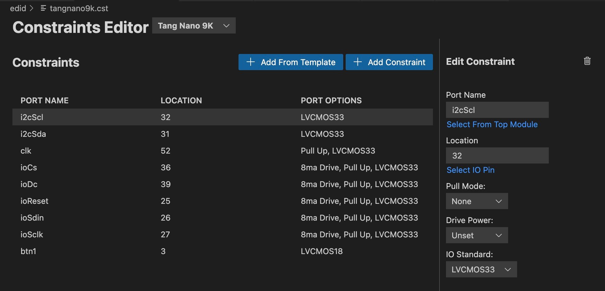
We have the clk signal and screen spi connection like usual, we also have 1 of the buttons hooked up and for the EDID connection we need two i2c ports 1 for the clock and 1 for data.
I chose pins 31 and 32 for no special reason other then them being consecutive and close to where I needed the signal to be on my breadboard but any of the 3.3 volt IOs would have worked.
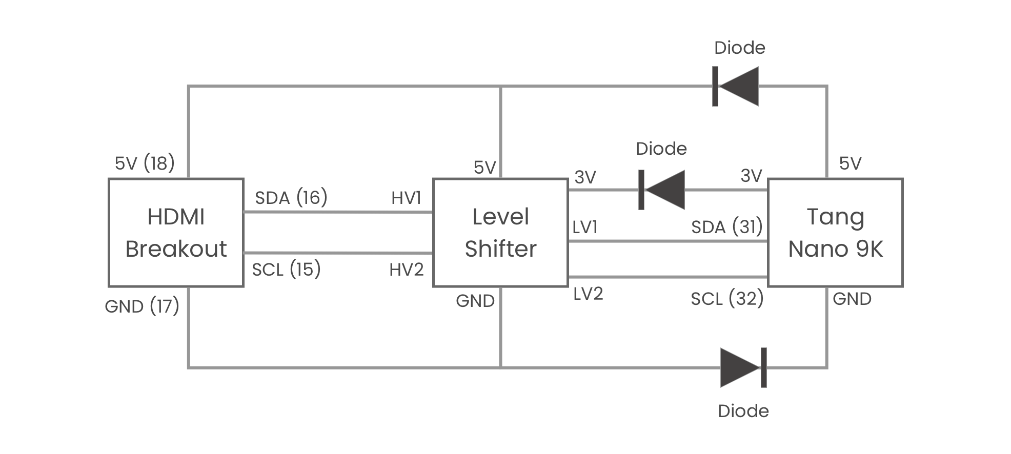
The last step is the electrical connection, and here there are a few things we need to deal with. The first issue, is that the DDC wires from the on-board HDMI connector are not connected to the FPGA, so we will need an alternate way of connecting these signals, and the second problem is that these signals are 5 volts and we are working with 3.3 volts.
For the first issue, there really aren't that many options, if you have a spare HDMI cable that you don't mind cutting up you can manually extract these two wires along with the 5V and ground lines for this interface. Another good option is by using an HDMI breakout board like the following:
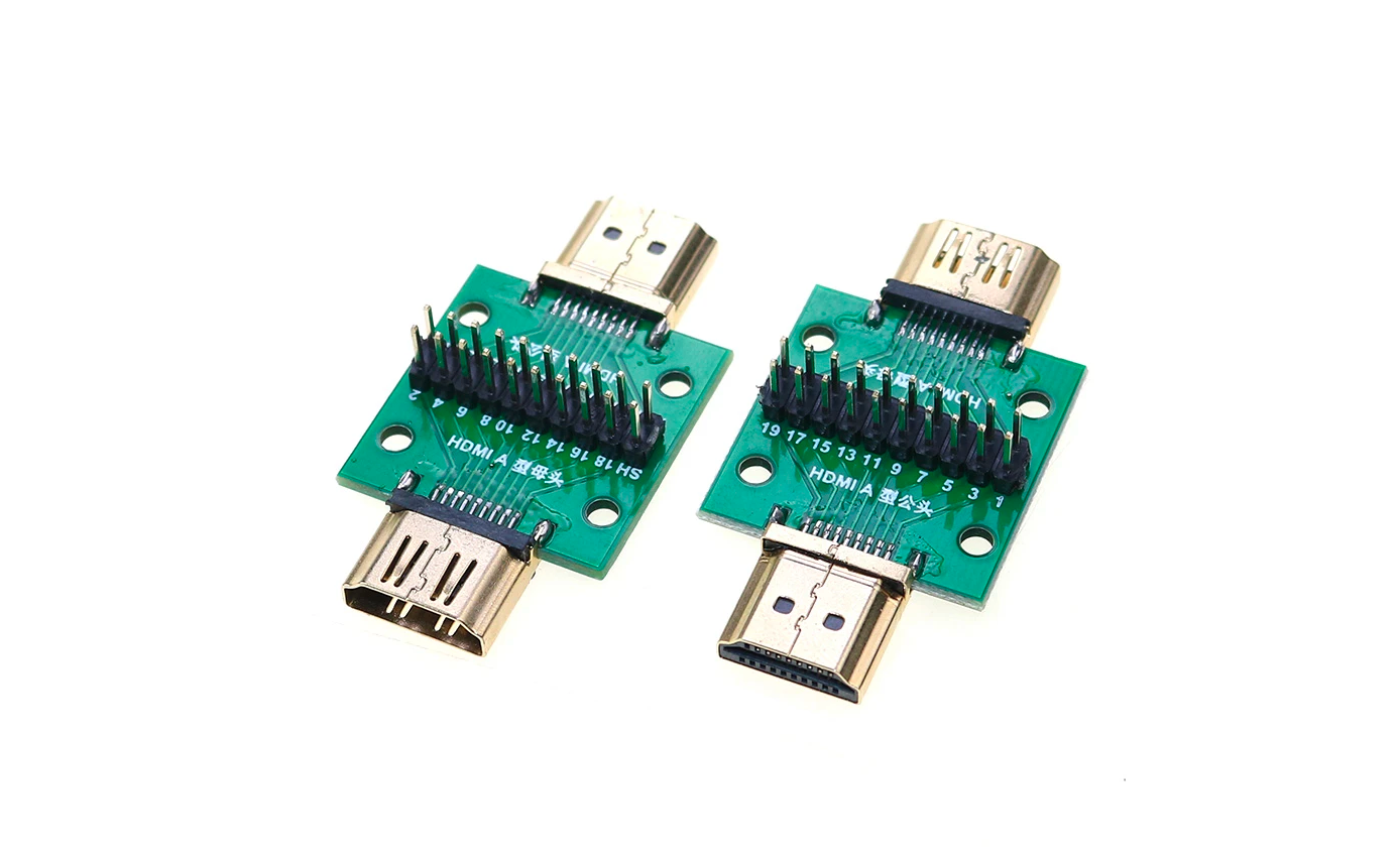
There are fancier ones out there with screw terminals or whatever, but I tested this generic passthrough one which only costs a dollar or two and I had no issues.
Using something like this you can easily extract pins 17 and 18 are the 5 volt and ground signal we need and pins 15 and 16 are the I2C signal (15 is the clock and 16 the data).
Next for the conversion from 3.3 volts to 5 volts we need some kind of level shifter. I2C uses pull-up resistors and each side can only pull the signal low, so there are simple 1 transistor solutions that do the conversion and you can get a board like the following:
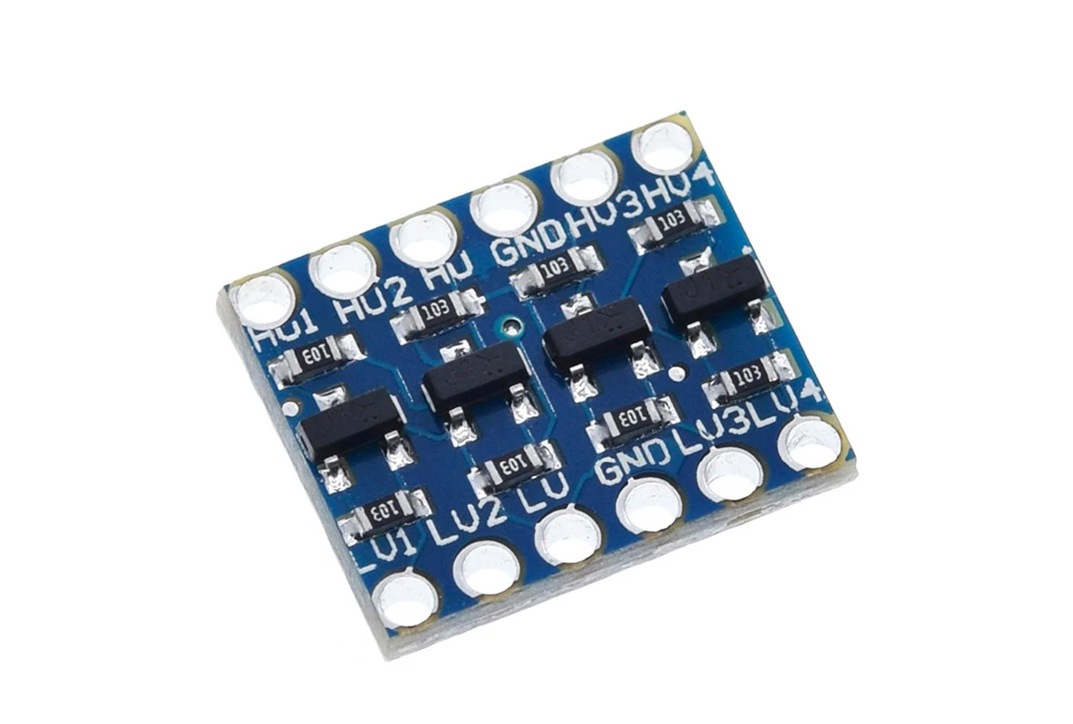
Which can convert up to 4 signals, the way it works is you power the HV (high voltage) pin with 5 volts and the LV pin with 3.3 volts, connect the grounds and then you can use each of the 4 channels to translate the voltage bidirectionally.
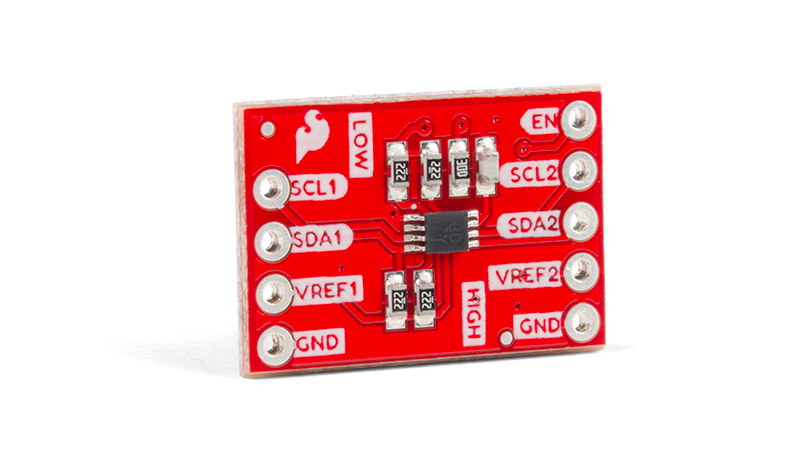
I ended up using a Sparkfun level shifter I had on-hand with a PCA9306 IC on-board to do the conversion:
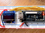
Other then that I also added some diodes to the 5v and 3.3v lines as-well as to the ground signal to protect the tang nano and make sure I wasn't getting current going from the 5v line to the 3.3v line (without the diodes I was getting some crossover causing the tang nano not to turn on, adding the diodes solved the issue). So with all the pieces in place you should have something like the following:
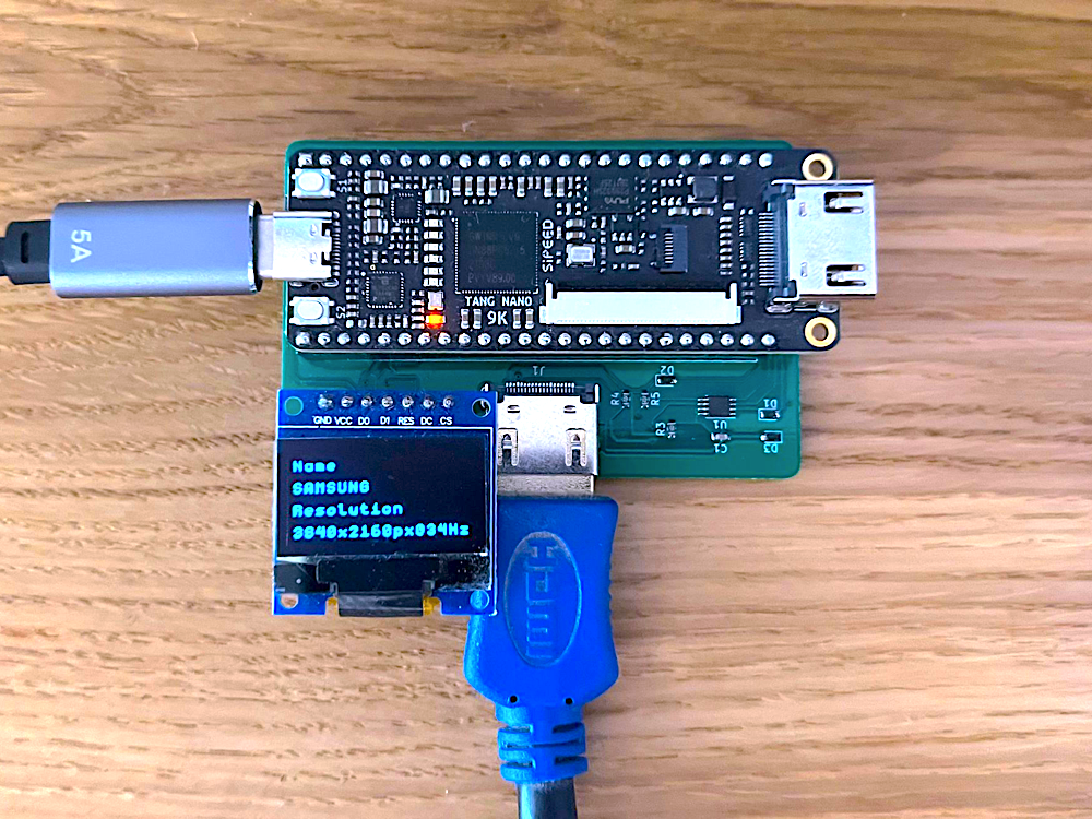
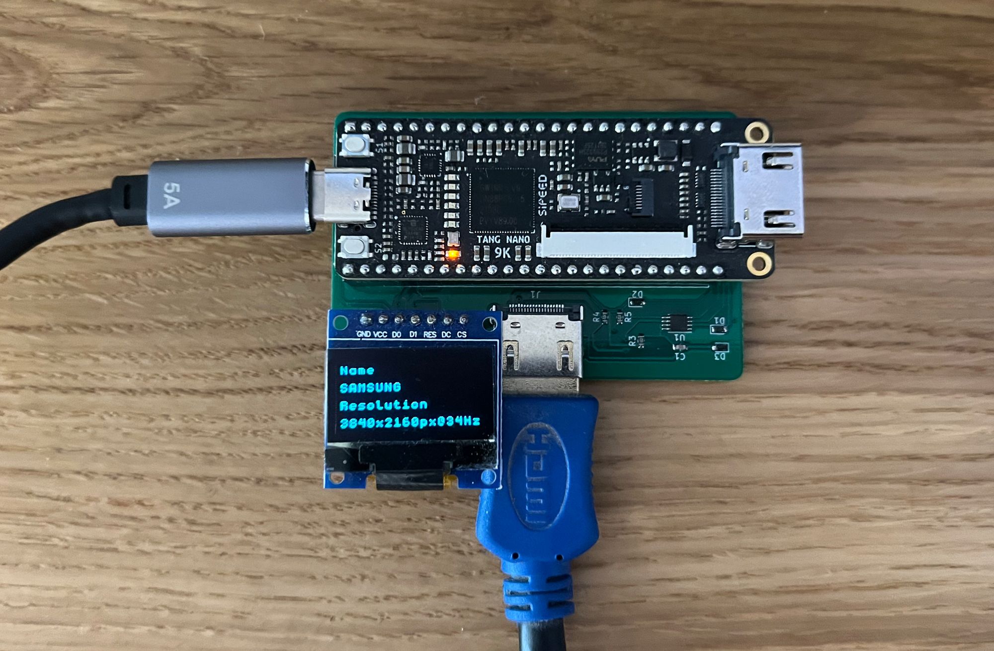
With that done you should be able to run the project and read the EDID info.
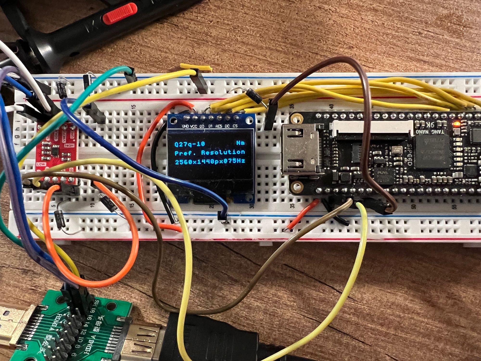
Don't get frightened by the mess of wires, this image was taken during a debug session where I was trying to find where the leak from 5 volts to the 3.3 volts was happening. hence the 5 diodes.
With a design that works, we decided to move everything over to a PCB to clean everything up. There isn't too much to go over here as its the same exact setup as above just without the wires
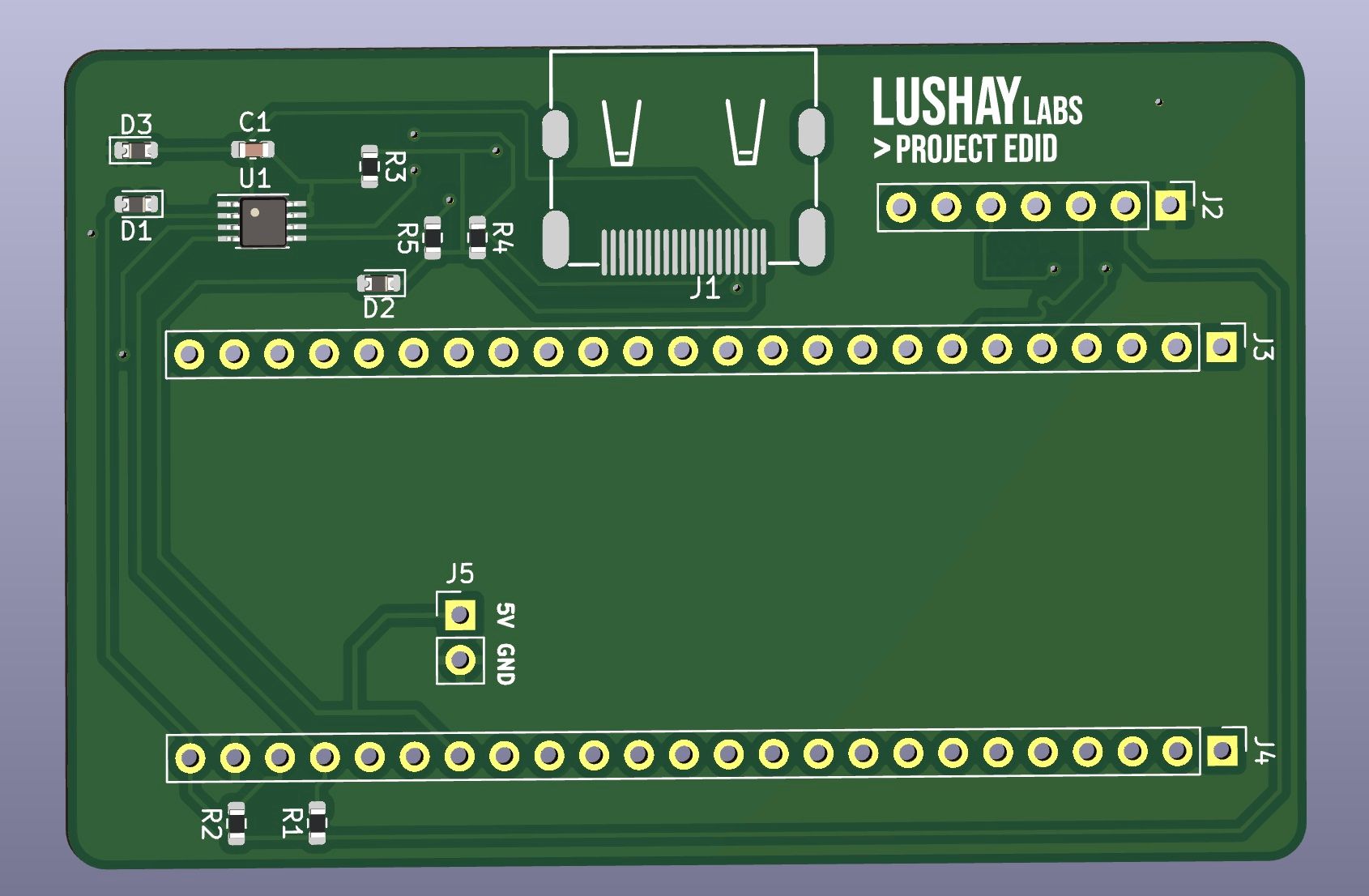
This was designed in KiCad and produced by PCBWay files and BOM are available from here
Running it with the PCB gives us something smaller than a credit card (if not measuring thickness) that allows us to read EDID info off any HDMI screen.
Conclusion
In this article we explored the EDID protocol and how to use the HDMIs I2C channel to retrieve this information. Thanks again to Jeroen and Martijn for all the help turning this idea into a functional "product" that could be used to solve a real world problem.
Thank you for reading, I hope you enjoyed the article, if you have any questions or comments feel free to leave them in the comments section below or PM us on Twitter @LushayLabs.
Like always the code is available in our TangNano series examples repo on github here.
